Philips Semiconductors
Product specification
Phase-locked loop
NE/SE564
APPLICATIONS
5V
FINE FREQUENCY
ADJUSTMENT
I
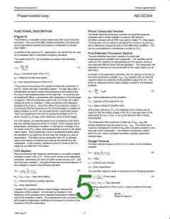
FM Demodulator
2
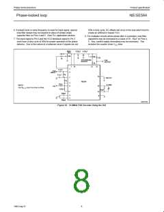
The NE564 can be used as an FM demodulator. The connections
for operation at 5V and 12V are shown in Figures 7 and 8,
respectively. The input signal is AC coupled with the output signal
being extracted at Pin 14. Loop filtering is provided by the
capacitors at Pins 4 and 5 with additional filtering being provided by
the capacitor at Pin 14. Since the conversion gain of the VCO is not
very high, to obtain sufficient demodulated output signal the
frequency deviation in the input signal should be 1% or higher.
2k
MODULATING
INPUT
1kHz
16
2
11
4
0.47µF
1kHz
6
7
5
15
14
1k
564
.01µF
3
1
Modulation Techniques
13
The NE564 phase-locked loop can be modulated at either the loop
filter ports (Pins 4 and 5) or the input port (Pin 6) as shown in Figure
9. The approximate modulation frequency can be determined from
the frequency conversion gain curve shown in Figure 10. This curve
will be appropriate for signals injected into Pins 4 and 5 as shown in
Figure 9.
8
10
9
12
80pF
f
= 5MHz
O
FREQUENCY SET CAP
5V
1k
MODULATED OUTPUT
(TTL)
5V
I
2
LOCK RANGE ADJUSTMENT
0.01µF
SR01033
Figure 9. Modulator
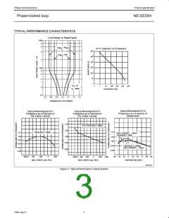
The lock range graph indicates that the +1.0MHz frequency
deviations will be within the lock range for input signal levels greater
than approximately 50mV with zero Pin 2 bias current. (While
strictly this figure is appropriate only for 50MHz, it can be used as a
LOOP FILTER
0.01µF
16
2
11
4
0.47µF
.01µF
FM INPUT
f
= 5MHz
6
7
5
O
M
1k
f
= 1kHz
ANALOG OUT
1kHz
guide for lock range estimates at other f ’ frequencies).
15
14
O
564
BIAS
FILTER
POST
DETECTION
FILTER
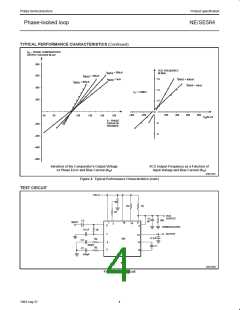
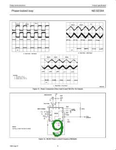
The hysteresis was adjusted experimentally via the 10kΩ
potentiometer and 2kΩ bias arrangement to give the waveshape
shown in Figure 12 for 20k, 500k, 2M baud rates with square wave
FSK modulation. Note the magnitude and phase relationships of the
phase comparators’ output voltages with respect to each other and
to the FSK output. The high-frequency sum components of the input
and VCO frequency also are viable as noise on the phase
comparator’s outputs.
3
1
0.1µF
13
8
10
9
12
80pF
f
= 5MHz
O
.01µF
FREQUENCY SET CAP
200
1k
OUTLINE OF SETUP PROCEDURE
12V
SR01032
1. Determine operating frequency of the VCO: IF÷ N in feedback
Figure 8. FM Demodulator at 12V
loop, then
FSK Demodulation
f = N x f .
O IN
The 564 PLL is particularly attractive for FSK demodulation since it
contains an internal voltage comparator and VCO which have TTL
compatible inputs and outputs, and it can operate from a single 5V
power supply. Demodulated DC voltages associated with the mark
and space frequencies are recovered with a single external
capacitor in a DC retriever without utilizing extensive filtering
networks. An internal comparator, acting as a Schmitt trigger with
an adjustable hysteresis, shapes the demodulated voltages into
compatible TTL output levels. The high-frequency design of the 564
enables it to demodulate FSK at high data rates in excess of 1.0M
baud.
2. Calculate value of the VCO frequency set capacitor:
1
C
O
2200 f
O
3. Set I (current sinking into Pin 2) for 100µA. After operation is
2
obtained, this value may be adjusted for best dynamic behavior,
VCC * 1.3V
and replace with fixed resistor value of R =
.
2
IB2
4. Check VCO output frequency with digital counter at Pin 9 of
device (loop open, VCO to φ det.). Adjust C trim or frequency
O
adj. Pins 4 - 5 for exact center frequency, if needed.
Figure 10 shows a high-frequency FSK decoder designed for input
frequency deviations of +1.0MHz centered around a free-running
frequency of 10.8MHz. the value of the timing capacitance required
was estimated from Figure 8 to be approximately 40pF. A trimmer
5. Close loop and inject input signal to Pin 6. Monitor Pins 3 and 6
with two-channel scope. Lock should occur with ∆φ
equal to
3 - 6
o
90 (phase error).
capacitor was added to fine tune f ’ 10.8MHz.
O
7
1994 Aug 31

 NXP [ NXP ]