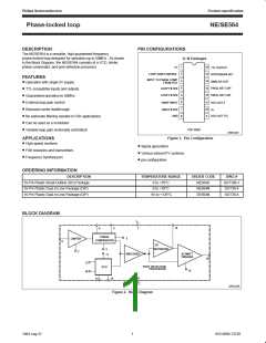
Philips Semiconductors
Product specification
Phase-locked loop
NE/SE564
FUNCTIONAL DESCRIPTION
Phase Comparator Section
The phase detection processor consists of a doubled-balanced
modulator with a limiter amplifier to improve AM rejection.
Schottky-clamped vertical PNPs are used to obtain TTL level inputs.
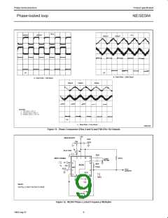
(Figure 6)
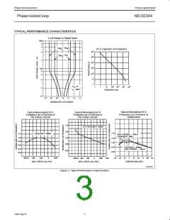
The NE564 is a monolithic phase-locked loop with a post detection
processor. The use of Schottky clamped transistors and optimized
device geometries extends the frequency of operation to greater
than 50MHz.
The loop gain can be varied by changing the current in Q and Q
which effectively changes the gain of the differential amplifiers. This
can be accomplished by introducing a current at Pin 2.
4
15
In addition to the classical PLL applications, the NE564 can be used
as a modulator with a controllable frequency deviation.
Post Detection Processor Section
The post detection processor consists of a unity gain
transconductance amplifier and comparator. The amplifier can be
used as a DC retriever for demodulation of FSK signals, and as a
post detection filter for linear FM demodulation. The comparator has
adjustable hysteresis so that phase jitter in the output signal can be
eliminated.
The output of the PLL can be written as shown in the following
equation:
(f - f )
IN
O
(1)
V
O
=
K
VCO
K
VCO
= conversion gain of the VCO
As shown in the equivalent schematic, the DC retriever is formed by
the transconductance amplifier Q - Q together with an external
42
43
f
f
= frequency of the input signal
IN
O
capacitor which is connected at the amplifier output (Pin 14). This
forms an integrator whose output voltage is shown in the following
equation:
= free-running frequency of the VCO
The process of recovering FSK signals involves the conversion of
the PLL output into logic compatible signals. For high data rates, a
considerable amount of carrier will be present at the output of the
PLL due to the wideband nature of the loop filter. To avoid the use
of complicated filters, a comparator with hysteresis or Schmitt trigger
is required. With the conversion gain of the VCO fixed, the output
voltage as given by Equation 1 varies according to the frequency
deviation of f from f . Since this differs from system to system, it
g
C
M
(3)
V
O
=
V dt
IN
2
g
M
= transconductance of the amplifier
C = capacitor at the output (Pin 14)
2
V
IN
= signal voltage at amplifier input
IN
O
is necessary that the hysteresis of the Schmitt trigger be capable of
being changed, so that it can be optimized for a particular system.
This is accomplished in the 564 by varying the voltage at Pin 15
which results in a change of the hysteresis of the Schmitt trigger.
With proper selection of C , the integrator time constant can be
2
varied so that the output voltage is the DC or average value of the
input signal for use in FSK, or as a post detection filter in linear
demodulation.
For FSK signals, an important factor to be considered is the drift in
the free-running frequency of the VCO itself. If this changes due to
temperature, according to Equation 1 it will lead to a change in the
DC levels of the PLL output, and consequently to errors in the digital
output signal. This is especially true for narrowband signals where
The comparator with hysteresis is made up of Q - Q with
49
50
positive feedback being provided by Q - Q . The hysteresis is
47
48
varied by changing the current in Q with a resulting variation in the
52
loop gain of the comparator. This method of hysteresis control,
which is a DC control, provides symmetric variation around the
nominal value.
the deviation in f itself may be less than the change in f due to
IN
O
temperature. This effect can be eliminated if the DC or average
value of the signal is retrieved and used as the reference to the
comparator. In this manner, variations in the DC levels of the PLL
output do not affect the FSK output.
Design Formula
The free-running frequency of the VCO is shown by the following
equation:
1
VCO Section
(4)
f
O
22 R (C + C )
Due to its inherent high-frequency performance, an emitter-coupled
oscillator is used in the VCO. In the circuit, shown in the equivalent
schematic, transistors Q21 and Q23 with current sources Q25 - Q26
form the basic oscillator. The approximate free-running frequency of
the oscillator is shown in the following equation:
C
1
S
R
= 100Ω
C
C = external cap in farads
1
C
= stray capacitance
S
1
(2)
f
O
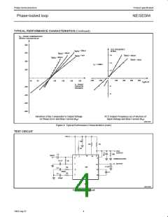
The loop filter diagram shown is explained by the following equation:
1
22 R (C + C )
C
1
S
(5)
f
S
=
(First Order)
R
= R = R = 100Ω (INTERNAL)
19 20
C
1 + sRC
3
C = external frequency setting capacitor
1
R = R = R = 1.3kΩ (Internal)*
12
13
C
= stray capacitance
S
By adding capacitors to Pins 4 and 5, a pole is added to the loop
transfer at
Variation of V (phase detector output voltage) changes the
D
frequency of the oscillator. As indicated by Equation 2, the
frequency of the oscillator has a negative temperature coefficient
due to the monolithic resistor. To compensate for this, a current I
1
RC
NOTE:
*Refer to Figure 6.
ω =
3
R
with negative temperature coefficient is introduced to achieve a low
frequency drift with temperature.
5
1994 Aug 31

 NXP [ NXP ]