Philips Semiconductors
Product specification
HEF4069UB
gates
Hex inverter
APPLICATION INFORMATION
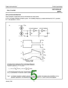
Some examples of applications for the HEF4069UB are shown below.
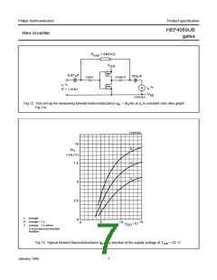
In Fig.7 an astable relaxation oscillator is given. The oscillation frequency is mainly determined by R1C1, provided
R1 << R2 and R2C2 << R1C1.
(a)
(b)
The function of R2 is to minimize the influence of the forward voltage across
the protection diodes on the frequency; C2 is a stray (parasitic) capacitance.
The period Tp is given by Tp = T1 + T2, in which
V
DD + VST
2 VDD – VST
---------------------------------
where
----------------------------
T1 = R1C1 In
and T2 = R1C1 In
VST
VDD – VST
VST is the signal threshold level of the inverter. The period is fairly independent
of VDD, VST and temperature. The duty factor, however, is influenced by VST
.
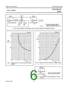
Fig.7 (a) Astable relaxation oscillator using two HEF4069UB inverters; the diodes may be BAW62; C2 is a
parasitic capacitance. (b) Waveforms at the points marked A, B, C and D in the circuit diagram.
January 1995
5

 NXP [ NXP ]