BT151-500R
NXP Semiconductors
SCR, 12 A, 15mA, 500 V, SOT78
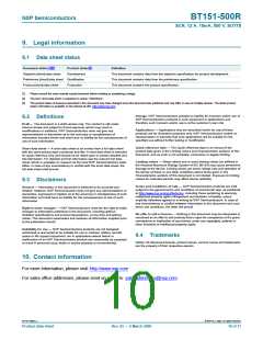
6. Characteristics
Table 6.
Symbol
Characteristics
Parameter
Conditions
Min
Typ
Max
Unit
Static characteristics
IGT
gate trigger current
VD = 12 V; Tj = 25 °C; IT = 100 mA; see
Figure 8
-
2
15
mA
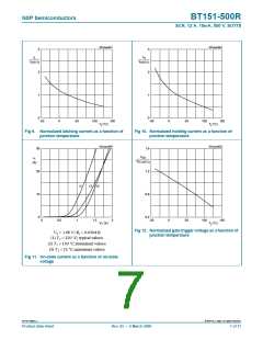
IL
latching current
holding current
on-state voltage
gate trigger voltage
VD = 12 V; Tj = 25 °C; see Figure 9
VD = 12 V; Tj = 25 °C; see Figure 10
IT = 23 A; Tj = 25 °C; see Figure 11
-
-
-
-
10
7
40
mA
mA
V
IH
20
VT
VGT
1.4
0.6
1.75
1.5
IT = 100 mA; VD = 12 V; Tj = 25 °C; see
Figure 12
V
IT = 100 mA; VD = 500 V; Tj = 125 °C
VD = 500 V; Tj = 125 °C
0.25
0.4
0.1
0.1
-
V
ID
IR
off-state current
reverse current
-
-
0.5
0.5
mA
mA
VR = 500 V; Tj = 125 °C
Dynamic characteristics
dVD/dt
rate of rise of off-state VDM = 335 V; Tj = 125 °C; exponential
50
130
1000
2
-
-
-
-
V/µs
V/µs
µs
voltage
waveform; gate open circuit
VDM = 335 V; Tj = 125 °C; RGK = 100 Ω;
exponential waveform; see Figure 7
200
tgt
tq
gate-controlled turn-on ITM = 40 A; VD = 500 V; IG = 100 mA;
-
-
time
dIG/dt = 5 A/µs; Tj = 25 °C
commutated turn-off
time
VDM = 335 V; Tj = 125 °C; ITM = 20 A;
VR = 25 V; (dIT/dt)M = 30 A/µs;
dVD/dt = 50 V/µs; RGK = 100 Ω
70
µs
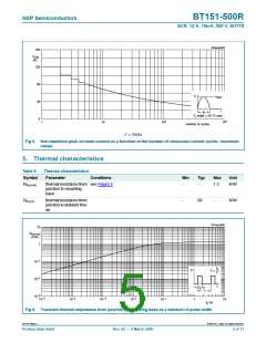
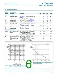
001aaa949
001aaa952
4
10
3
I
GT
dV /dt
D
(V/μs)
I
GT(25°C)
(1)
(2)
3
10
2
2
10
1
10
0
−50
0
50
100
150
0
50
100
150
T (°C)
j
T (°C)
j
Fig 8. Normalized gate trigger current as a function of
junction temperature
Fig 7. Critical rate of rise of off-state voltage as a
function of junction temperature; minimum
values
BT151-500R_5
© NXP B.V. 2009. All rights reserved.
Product data sheet
Rev. 05 — 2 March 2009
6 of 11

 NXP [ NXP ]