BT151-500R
NXP Semiconductors
SCR, 12 A, 15mA, 500 V, SOT78
4. Limiting values
Table 4.
Limiting values
In accordance with the Absolute Maximum Rating System (IEC 60134).
Symbol
Parameter
Conditions
Min
Max
Unit
VDRM
repetitive peak off-state
voltage
-
500
V
VRRM
IT(AV)
repetitive peak reverse
voltage
-
-
-
-
500
7.5
12
V
average on-state
current
half sine wave; Tmb ≤ 109 °C; see Figure 3
A
IT(RMS)
dIT/dt
RMS on-state current
half sine wave; Tmb ≤ 109 °C; see Figure 1; see
Figure 2
A
rate of rise of on-state IT = 20 A; IG = 50 mA; dIG/dt = 50 mA/µs
current
50
A/µs
IGM
PGM
Tstg
Tj
peak gate current
peak gate power
-
2
A
-
5
W
°C
°C
A
storage temperature
junction temperature
-40
150
125
132
120
-
-
-
ITSM
non-repetitive peak
on-state current
half sine wave; tp = 8.3 ms; Tj(init) = 25 °C
half sine wave; tp = 10 ms; Tj(init) = 25 °C; see
Figure 4; see Figure 5
A
I2t
I2t for fusing
tp = 10 ms; sine-wave pulse
over any 20 ms period
-
-
-
72
0.5
5
A2s
W
PG(AV)
VRGM
average gate power
peak reverse gate
voltage
V
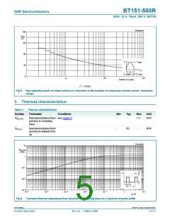
001aaa954
001aaa999
25
16
I
T(RMS)
(A)
I
T(RMS)
(A)
20
15
10
5
12
8
4
0
10
0
−50
−2
−1
10
1
10
0
50
100
150
surge duration (s)
T
mb
(°C)
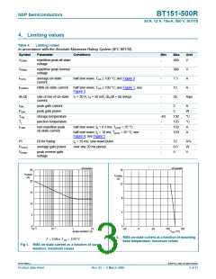
Fig 2. RMS on-state current as a function of mounting
base temperature; maximum values
Fig 1. RMS on-state current as a function of surge
duration; maximum values
BT151-500R_5
© NXP B.V. 2009. All rights reserved.
Product data sheet
Rev. 05 — 2 March 2009
3 of 11

 NXP [ NXP ]