Philips Semiconductors
Product data
Single wire CAN transceiver
AU5790
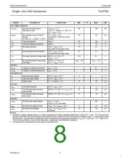
SYMBOL
PARAMETER
CONDITIONS
MIN.
TYP.
MAX.
UNIT
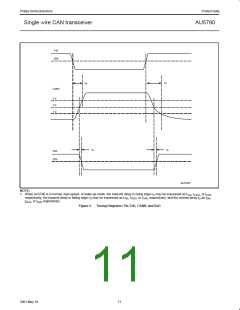
Pin TxD (continued)
t
Transmit delay in high-speed
mode, bus rising edge
NSTB = 5 V, EN = 0 V;
0.1
1.5
µs
TrHS
R = 100 Ω, C = 15 nF;
L
L
8 V < V
< 16 V;
BAT
measured from the falling edge on
TxD to V = 3.0 V
CANH
t
Transmit delay in high-speed
mode, bus falling edge
NSTB = 5 V, EN = 0 V;
0.2
3
µs
TfHS
R = 100 Ω, C = 15 nF;
L
L
8 V < V
< 16 V;
BAT
measured from the rising edge on
TxD to V = 1.0 V
CANH
Pin RxD
t
t
t
t
Receive delay in normal mode,
bus rising and falling edge
NSTB = 5 V, EN = 5 V;
5.5 V < V < 27 V;
0.3
0.3
0.3
10
1
1
µs
µs
µs
µs
DN
BAT
CANH to RxD time measured from
= 2.0 V to V = 2.5 V
V
CANH
RxD
Receive delay in wake-up mode,
bus rising and falling edge
NSTB = 0 V, EN = 5 V;
5.5 V < V < 27 V;
DW
DHS
DS
BAT
CANH to RxD time measured from
= 2.0 V to V = 2.5 V
V
CANH
RxD
Receive delay in high-speed
mode, bus rising and falling edge
NSTB = 5 V, EN = 0 V;
8 V < V < 16 V;
1
BAT
CANH to RxD time measured from
= 2.0 V to V = 2.5 V
V
CANH
RxD
Receive delay in sleep mode,
bus rising edge
NSTB = 0 V, EN = 0 V;
CANH to RxD time, measured from
= min {(V – 3.78 V),
70
V
CANH
BAT
7.13 V} to V
= 2.5 V
RxD
NOTES:
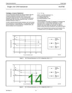
1. Operation at battery voltages down to 5.3 volts is guaranteed by design. Operation higher than 18 volts (18 V < V
< 27 V) for up to two
BAT
minutes is permitted if the thermal design of the board prevents reaching the thermal protection temperature limit, T , otherwise the device
sd
will self protect. Typically these requirements will be encountered during jump start operation at T
85 °C and V
< 27 V. Refer to the
amb
BAT
“Thermal Characteristics” section of this data sheet, or application note AN2005 for guidance.
2. This parameter is characterized but not subject to production test.
10
2001 May 18

 NXP [ NXP ]