74LVC14A
Philips Semiconductors
Hex inverting Schmitt trigger with 5 V tolerant input
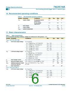
Table 7:
Static characteristics …continued
At recommended operating conditions; voltages are referenced to GND (ground = 0 V).
Symbol Parameter
Conditions
Min
Typ
Max
Unit
VOL
LOW-level voltage output
VI = VIH or VIL
IO = 100 µA; VCC = 2.7 V to 3.6 V
IO = 8 mA; VCC = 2.3 V to 2.7 V
IO = 12 mA; VCC = 2.7 V
IO = 24 mA; VCC = 3.0 V
VCC = 3.6 V; VI = 5.5 V or GND
VCC = 3.6 V; VI = VCC or GND; IO = 0 A
-
-
-
-
-
-
-
-
-
-
-
-
-
-
0.3
0.75
0.6
0.8
±20
40
V
V
V
V
ILI
input leakage current
µA
µA
mA
ICC
∆ICC
quiescent supply current
additional quiescent supply VCC = 2.7 V to 3.6 V; VI = VCC − 0.6 V;
current per input pin IO = 0 A
5
[1] All typical values are measured at Tamb = 25 °C.
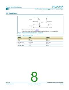
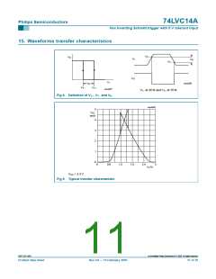
12. Dynamic characteristics
Table 8:
Dynamic characteristics
Voltages are referenced to GND (ground = 0 V); for test circuit see Figure 7.
Symbol Parameter
Conditions
Min
Typ
Max
Unit
Tamb = −40 °C to +85 °C[1]
tPHL
tPLH
,
propagation delay nA to nY
see Figure 6
VCC = 1.2 V
-
16
4.0
3.6
3.2
-
-
ns
ns
ns
ns
ns
pF
VCC = 2.3 V to 2.7 V
VCC = 2.7 V
1.5
1.5
1.0
-
7.8
7.5
6.4
1.0
-
VCC = 3.0 V to 3.6 V
[2]
tsk(0)
CPD
skew
power dissipation capacitance VCC = 3.3 V
[3] [4]
-
10
Tamb = −40 °C to +125 °C
tPHL propagation delay nA to nY
tPLH
,
see Figure 6
VCC = 1.2 V
-
-
-
-
-
-
-
ns
ns
ns
ns
ns
VCC = 2.3 V to 2.7 V
VCC = 2.7 V
1.5
1.5
1.0
-
10.0
9.5
8.0
1.5
VCC = 3.0 V to 3.6 V
[2]
tsk(0)
skew
[1] All typical values are measured at nominal VCC and Tamb = 25 °C.
[2] Skew between any two outputs of the same package switching in the same direction. This parameter is guaranteed by design.
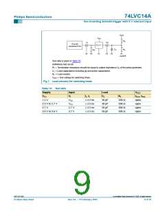
[3] CPD is used to determine the dynamic power dissipation (PD in µW).
PD = CPD × VCC2 × fi × N + Σ(CL × VCC2 × fo) where:
fi = input frequency in MHz;
fo = output frequency in MHz;
CL = output load capacitance in pF;
VCC = supply voltage in V;
N = number of inputs switching;
Σ(CL × VCC2 × fo) = sum of the outputs.
[4] The condition is VI = GND to VCC
.
9397 750 14591
© Koninklijke Philips Electronics N.V. 2005. All rights reserved.
Product data sheet
Rev. 04 — 15 February 2005
7 of 19

 NXP [ NXP ]