74LVC14A
Philips Semiconductors
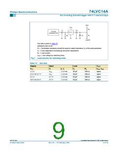
Hex inverting Schmitt trigger with 5 V tolerant input
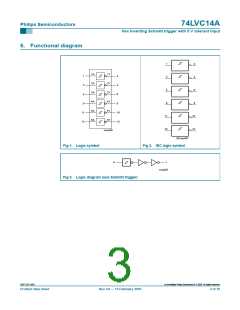
8. Functional description
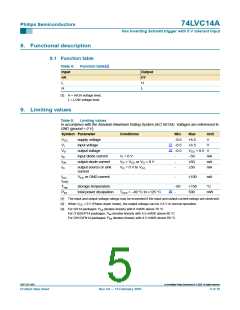
8.1 Function table
Table 4:
Function table[1]
Input
nA
L
Output
nY
H
H
L
[1] H = HIGH voltage level;
L = LOW voltage level.
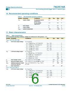
9. Limiting values
Table 5:
Limiting values
In accordance with the Absolute Maximum Rating System (IEC 60134). Voltages are referenced to
GND (ground = 0 V).
Symbol Parameter
Conditions
Min
−0.5
−0.5
−0.5
-
Max
+6.5
+6.5
Unit
V
VCC
VI
supply voltage
[1]
[1]
input voltage
V
VO
IIK
output voltage
VCC + 0.5 V
input diode current
output diode current
VI < 0 V
−50
±50
±50
mA
IOK
IO
VO > VCC or VO < 0 V
VO = 0 V to VCC
-
mA
mA
output source or sink
current
-
ICC
,
VCC or GND current
-
±100
mA
IGND
Tstg
Ptot
storage temperature
total power dissipation
−65
+150
500
°C
[3]
Tamb = −40 °C to +125 °C
-
mW
[1] The input and output voltage ratings may be exceeded if the input and output current ratings are observed.
[2] When VCC = 0 V (Power-down mode), the output voltage can be 3.6 V in normal operation.
[3] For SO14 packages: Ptot derates linearly with 8 mW/K above 70 °C.
For (T)SSOP14 packages: Ptot derates linearly with 5.5 mW/K above 60 °C.
For DHVQFN14 packages: Ptot derates linearly with 4.5 mW/K above 60 °C.
9397 750 14591
© Koninklijke Philips Electronics N.V. 2005. All rights reserved.
Product data sheet
Rev. 04 — 15 February 2005
5 of 19

 NXP [ NXP ]