Philips Semiconductors
Product specification
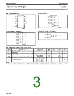
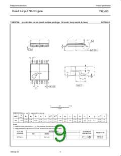
Quad 2-input NAND gate
74LV00
1, 2
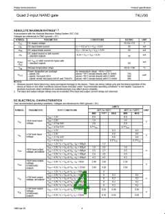
ABSOLUTE MAXIMUM RATINGS
In accordance with the Absolute Maximum Rating System (IEC 134).
Voltages are referenced to GND (ground = 0V).
SYMBOL
PARAMETER
DC supply voltage
CONDITIONS
RATING
UNIT
V
V
CC
–0.5 to +7.0
±I
DC input diode current
DC output diode current
V < –0.5 or V > V + 0.5V
20
50
mA
mA
IK
I
I
CC
±I
OK
V
O
< –0.5 or V > V + 0.5V
O
CC
DC output source or sink current
– standard outputs
±I
O
–0.5V < V < V + 0.5V
mA
O
CC
25
DC V or GND current for types with
– standard outputs
CC
±I
±I
,
mA
GND
50
CC
T
stg
Storage temperature range
–65 to +150
°C
Power dissipation per package
– plastic DIL
– plastic mini-pack (SO)
for temperature range: –40 to +125°C
above +70°C derate linearly with 12 mW/K
above +70°C derate linearly with 8 mW/K
above +60°C derate linearly with 5.5 mW/K
750
500
400
P
TOT
mW
– plastic shrink mini-pack (SSOP and TSSOP)
NOTES:
1. Stresses beyond those listed may cause permanent damage to the device. These are stress ratings only and functional operation of the
device at these or any other conditions beyond those indicated under “recommended operating conditions” is not implied. Exposure to
absolute-maximum-rated conditions for extended periods may affect device reliability.
2. The input and output voltage ratings may be exceeded if the input and output current ratings are observed.
DC ELECTRICAL CHARACTERISTICS
Over recommended operating conditions. Voltages are referenced to GND (ground = 0V).
LIMITS
-40°C to +85°C
-40°C to +125°C
SYMBOL
PARAMETER
TEST CONDITIONS
= 1.2V
UNIT
1
MIN
0.9
1.4
2.0
TYP
MAX
MIN
0.9
1.4
2.0
MAX
V
V
V
V
V
V
V
V
V
V
V
V
V
CC
CC
CC
CC
CC
CC
CC
CC
CC
CC
CC
CC
CC
= 2.0V
HIGH level Input
voltage
V
IH
V
= 2.7 to 3.6V
= 4.5 to 5.5V
= 1.2V
0.7*V
0.7*V
CC
CC
0.3
0.6
0.8
0.3
0.6
0.8
= 2.0V
LOW level Input
voltage
V
IL
V
= 2.7 to 3.6V
= 4.5 to 5.5
0.3*V
0.3*V
CC
CC
= 1.2V; V = V or V –I = 100µA
1.2
2.0
2.7
3.0
4.5
I
IH
IL;
O
= 2.0V; V = V or V –I = 100µA
1.8
2.5
2.8
4.3
1.8
2.5
2.8
4.3
I
IH
IL;
O
HIGH level output
voltage; all outputs
= 2.7V; V = V or V –I = 100µA
V
V
V
V
V
V
I
IH
IL;
O
OH
= 3.0V; V = V or V –I = 100µA
I
IH
IL;
O
= 4.5V; V = V or V –I = 100µA
I
IH
IL;
O
HIGH level output
voltage;
STANDARD
V
V
= 3.0V; V = V or V –I = 6mA
2.40
3.60
2.82
4.20
2.20
3.50
CC
I
IH
IL;
O
OH
= 4.5V; V = V or V –I = 12mA
CC
I
IH
IL;
O
outputs
V
CC
V
CC
V
CC
V
CC
V
CC
= 1.2V; V = V or V I
IL; O
= 100µA
= 100µA
= 100µA
= 100µA
= 100µA
0
0
0
0
0
I
IH
= 2.0V; V = V or V
I
0.2
0.2
0.2
0.2
0.2
0.2
0.2
0.2
I
IH
IL; O
LOW level output
= 2.7V; V = V or V
I
V
V
I
IH
IL; O
OL
= 3.0V; V = V or V I
IL; O
I
IH
= 4.5V; V = V or V I
IL; O
I
IH
LOW level output
voltage;
STANDARD
V
= 3.0V; V = V or V I = 6mA
IL; O
0.25
0.35
0.40
0.55
0.50
0.65
CC
CC
I
IH
OL
V
= 4.5V; V = V or V I = 12mA
IL; O
I
IH
outputs
4
1998 Apr 20

 NXP [ NXP ]