Philips Semiconductors
Product specification
Quad 2-input NAND gate
74LV00
FEATURES
• Wide operating voltage: 1.0 to 5.5 V
• Optimized for low voltage applications: 1.0 to 3.6 V
DESCRIPTION
The 74LV00 is a low-voltage Si-gate CMOS device that is pin and
function compatible with 74HC/HCT00.
The 74LV00 provides the 2-input NAND function.
• Accepts TTL input levels between V = 2.7 V and V = 3.6 V
CC
CC
• Typical V
(output ground bounce) < 0.8 V at V = 3.3 V,
OLP
= 25°C
CC
T
amb
• Typical V
(output V undershoot) > 2 V at V = 3.3 V,
OHV
= 25°C
OH
CC
T
amb
• Output capability: standard
• I category: SSI
CC
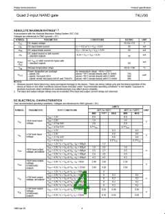
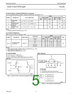
QUICK REFERENCE DATA
GND = 0 V; T
= 25°C; t =t ≤ 2.5 ns
amb
r f
SYMBOL
PARAMETER
CONDITIONS
TYPICAL
UNIT
Propagation delay
nA, nB to nY
C = 15 pF;
L
t
/t
7
ns
PHL PLH
V
CC
= 3.3 V
C
Input capacitance
3.5
22
pF
pF
I
C
Power dissipation capacitance per gate
See Notes 1 and 2
PD
NOTES:
1. C is used to determine the dynamic power dissipation (P in µW)
PD
D
2
2
P
= C V
f )ȍ (C V
f ) where:
D
PD
CC
i
L
CC o
f = input frequency in MHz; C = output load capacitance in pF;
i
L
f = output frequency in MHz; V = supply voltage in V;
o
CC
2
ȍ (C V
f ) = sum of the outputs.
L
CC
o
2. The condition is V = GND to V
I
CC.
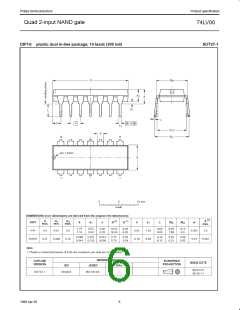
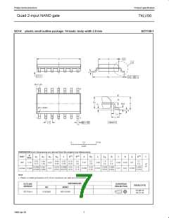
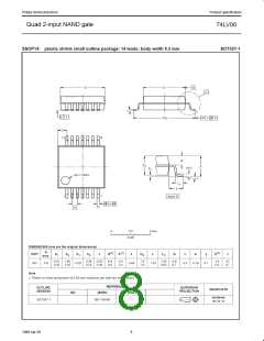
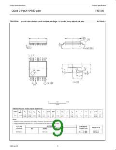
ORDERING INFORMATION
PACKAGES
TEMPERATURE RANGE OUTSIDE NORTH AMERICA
NORTH AMERICA
74LV00 N
PKG. DWG. #
SOT27-1
14-Pin Plastic DIL
–40°C to +125°C
–40°C to +125°C
–40°C to +125°C
–40°C to +125°C
74LV00 N
74LV00 D
14-Pin Plastic SO
74LV00 D
SOT108-1
SOT337-1
SOT402-1
14-Pin Plastic SSOP Type II
14-Pin Plastic TSSOP Type I
74LV00 DB
74LV00 PW
74LV00 DB
74LV00PW DH
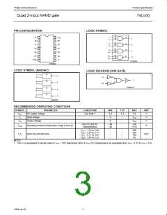
PIN DESCRIPTION
FUNCTION TABLE
PIN
INPUTS
OUTPUTS
nY
SYMBOL
NUMBER
FUNCTION
nA
nB
1, 4, 9, 12
1A – 4A Data inputs
L
L
L
H
L
H
H
H
2, 5, 10, 13 1B – 4B Data inputs
3, 6, 8, 11
1Y – 4Y Data outputs
GND Ground (0 V)
Positive supply voltage
H
7
H
H
L
14
V
CC
NOTES:
H = HIGH voltage level
L
= LOW voltage level
2
1998 Apr 20
853–1898 19257

 NXP [ NXP ]