74HC86; 74HCT86
NXP Semiconductors
Quad 2-input EXCLUSIVE-OR gate
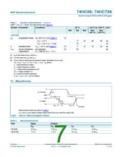
Table 7.
Dynamic characteristics …continued
GND = 0 V; CL = 50 pF; for load circuit see Figure 6.
Symbol Parameter
Conditions
25 C
40 C to +125 C Unit
Max Max
(85 C) (125 C)
Min
Typ
Max
74HCT86
[1]
tpd
propagation delay nA, nB to nY; see Figure 5
VCC = 4.5 V
-
-
-
-
17
14
7
32
-
40
-
48
-
ns
ns
ns
pF
VCC = 5.0 V; CL = 15 pF
[2]
[3]
tt
transition time
power dissipation per package;
capacitance VI = GND to VCC 1.5 V
VCC = 4.5 V; see Figure 5
15
-
19
-
22
-
CPD
30
[1] tpd is the same as tPHL and tPLH
.
[2] tt is the same as tTHL and tTLH
.
[3] CPD is used to determine the dynamic power dissipation (PD in W):
PD = CPD VCC2 fi N + (CL VCC2 fo) where:
fi = input frequency in MHz;
fo = output frequency in MHz;
CL = output load capacitance in pF;
VCC = supply voltage in V;
N = number of inputs switching;
(CL VCC2 fo) = sum of outputs.
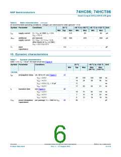
11. Waveforms
V
I
nA, nB input
GND
V
M
t
t
PLH
PHL
V
OH
V
Y
V
nY output
M
V
X
V
OL
t
t
TLH
THL
001aai814
Measurement points are given in Table 9.
OL and VOH are typical voltage output levels that occur with the output load.
V
Fig 5. Input to output propagation delays
Table 8.
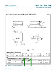
Type
Measurement points
Input
VM
Output
VM
VX
VY
74HC86
0.5VCC
1.3 V
0.5VCC
1.3 V
0.1VCC
0.1VCC
0.9VCC
0.9VCC
74HCT86
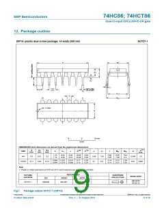
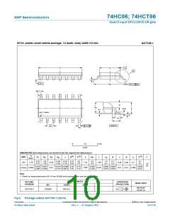
74HC_HCT86
All information provided in this document is subject to legal disclaimers.
© NXP B.V. 2012. All rights reserved.
Product data sheet
Rev. 3 — 27 August 2012
7 of 16

 NXP [ NXP ]