74HC86; 74HCT86
NXP Semiconductors
Quad 2-input EXCLUSIVE-OR gate
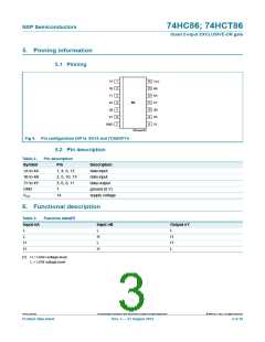
5. Pinning information
5.1 Pinning
1
2
3
4
5
6
7
14
13
12
11
10
9
1A
1B
V
CC
4B
4A
4Y
3B
3A
3Y
1Y
2A
86
2B
2Y
8
GND
001aad103
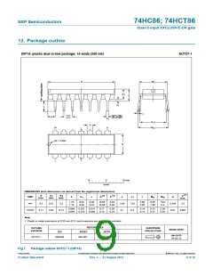
Fig 4. Pin configuration DIP14, SO14 and (T)SSOP14
5.2 Pin description
Table 2.
Symbol
1A to 4A
1B to 4B
1Y to 4Y
GND
Pin description
Pin
Description
data input
1, 4, 9, 12
2, 5, 10, 13
3, 6, 8, 11
7
data input
data output
ground (0 V)
supply voltage
VCC
14
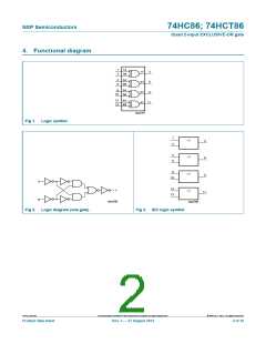
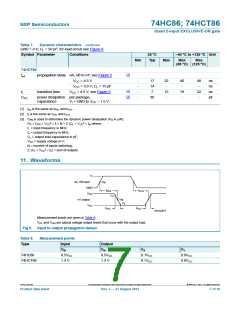
6. Functional description
Table 3.
Function table[1]
Input nA
Input nB
Output nY
L
L
L
L
H
L
H
H
L
H
H
H
[1] H = HIGH voltage level;
L = LOW voltage level.
74HC_HCT86
All information provided in this document is subject to legal disclaimers.
© NXP B.V. 2012. All rights reserved.
Product data sheet
Rev. 3 — 27 August 2012
3 of 16

 NXP [ NXP ]