Philips Semiconductors
Product specification
Octal D-type flip-flop with reset;
positive-edge trigger
74HC/HCT273
AC WAVEFORMS
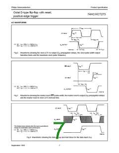
(1) HC : VM = 50%; VI = GND to VCC
.
HCT: VM = 1.3 V; VI = GND to 3 V.
Fig.6 Waveforms showing the clock (CP) to output (Qn) propagation delays, the clock pulse width output
transition times and the maximum clock pulse frequency.
(1) HC : VM = 50%; VI = GND to VCC
.
HCT: VM = 1.3 V; VI = GND to 3 V.
Fig.7 Waveforms showing the master reset (MR) pulse width, the master reset to output (Qn) propagation delays
and the master reset to clock (CP) removal time.
The shaded areas indicate when the input is permitted to
change for predictable output performance.
(1) HC : VM = 50%; VI = GND to VCC
.
HCT: VM = 1.3 V; VI = GND to 3 V.
Fig.8 Waveforms showing the data set-up and hold times for the data input (Dn).
September 1993
7

 NXP [ NXP ]