Philips Semiconductors
Product specification
Octal D-type flip-flop with reset;
positive-edge trigger
74HC/HCT273
FEATURES
GENERAL DESCRIPTION
• Ideal buffer for MOS microprocessor or memory
• Common clock and master reset
• Eight positive edge-triggered D-type flip-flops
• See “377” for clock enable version
• See “373” for transparent latch version
• See “374” for 3-state version
The 74HC/HCT273 are high-speed Si-gate CMOS devices
and are pin compatible with low power Schottky TTL
(LSTTL). They are specified in compliance with JEDEC
standard no. 7A.
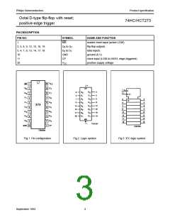
The 74HC/HCT273 have eight edge-triggered, D-type
flip-flops with individual D inputs and Q outputs. The
common clock (CP) and master reset (MR) inputs load and
reset (clear) all flip-flops simultaneously.
The state of each D input, one set-up time before the
LOW-to-HIGH clock transition, is transferred to the
corresponding output (Qn) of the flip-flop.
• Output capability; standard
• ICC category: MSI
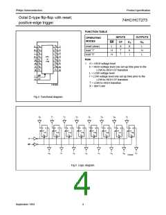
All outputs will be forced LOW independently of clock or
data inputs by a LOW voltage level on the MR input.
The device is useful for applications where the true output
only is required and the clock and master reset are
common to all storage elements.
QUICK REFERENCE DATA
GND = 0 V; Tamb = 25 °C; tr = tf = 6 ns
TYPICAL
SYMBOL
PARAMETER
CONDITIONS
UNIT
HC
HCT
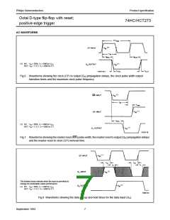
tPHL/ tPLH
propagation delay
CL = 15 pF; VCC = 5 V
CP to Qn
15
15
66
3.5
20
15
20
36
3.5
23
ns
MR to Qn
ns
fmax
CI
maximum clock frequency
input capacitance
MHz
pF
CPD
power dissipation capacitance per flip-flop
notes 1 and 2
pF
Notes
1. CPD is used to determine the dynamic power dissipation (PD in µW):
2
PD = CPD × VCC2 × fi + ∑ (CL × VCC × fo) where:
fi = input frequency in MHz
fo = output frequency in MHz
∑ (CL × VCC2 × fo) = sum of outputs
CL = output load capacitance in pF
VCC = supply voltage in V
2. For HC the condition is VI = GND to VCC
For HCT the condition is VI = GND to VCC − 1.5 V
ORDERING INFORMATION
See “74HC/HCT/HCU/HCMOS Logic Package Information”.
September 1993
2

 NXP [ NXP ]