Philips Semiconductors
Product specification
Hex inverter
74HC04; 74HCT04
FEATURES
DESCRIPTION
• Complies with JEDEC standard no. 8-1A
The 74HC/HCT04 are high-speed Si-gate CMOS devices
and are pin compatible with low power Schottky TTL
(LSTTL). They are specified in compliance with JEDEC
standard no. 7A. The 74HC/HCT04 provide six inverting
buffers.
• ESD protection:
HBM EIA/JESD22-A114-A exceeds 2000 V
MM EIA/JESD22-A115-A exceeds 200 V.
• Specified from −40 to +85 °C and −40 to +125 °C.
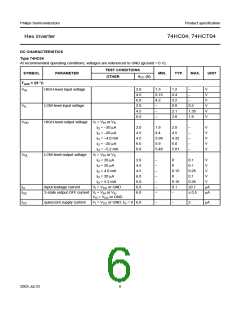
QUICK REFERENCE DATA
GND = 0 V; Tamb = 25 °C; tr = tf ≤ 6.0 ns.
TYPICAL
SYMBOL
PARAMETER
CONDITIONS
UNIT
HC04
HCT04
t
PHL/tPLH propagation delay nA to nY
CL = 15 pF; VCC = 5 V
7
8
ns
pF
pF
CI
input capacitance
power dissipation capacitance per gate notes 1 and 2
3.5
21
3.5
24
CPD
Notes
1. CPD is used to determine the dynamic power dissipation (PD in µW).
PD = CPD × VCC2 × fi × N + Σ(CL × VCC2 × fo) where:
fi = input frequency in MHz;
fo = output frequency in MHz;
CL = output load capacitance in pF;
VCC = supply voltage in Volts;
N = total load switching outputs;
Σ(CL × VCC2 × fo) = sum of the outputs.
2. For 74HC04: the condition is VI = GND to VCC
.
For 74HCT04: the condition is VI = GND to VCC − 1.5 V.
FUNCTION TABLE
See note 1.
INPUT
nA
OUTPUT
nY
L
H
L
H
Note
1. H = HIGH voltage level;
L = LOW voltage level.
2003 Jul 23
2

 NXP [ NXP ]