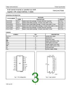
Philips Semiconductors
Product specification
8-bit serial-in/serial or parallel-out shift
register with output latches; 3-state
74HC/HCT595
FEATURES
DESCRIPTION
• 8-bit serial input
The 74HC/HCT595 are high-speed Si-gate CMOS devices
and are pin compatible with low power Schottky TTL
(LSTTL). They are specified in compliance with JEDEC
standard no. 7A.
• 8-bit serial or parallel output
• Storage register with 3-state outputs
• Shift register with direct clear
• 100 MHz (typ) shift out frequency
• Output capability:
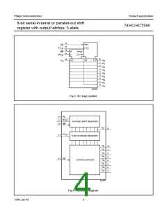
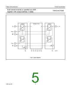
The “595” is an 8-stage serial shift register with a storage
register and 3-state outputs. The shift register and storage
register have separate clocks.
– parallel outputs; bus driver
– serial output; standard
• ICC category: MSI.
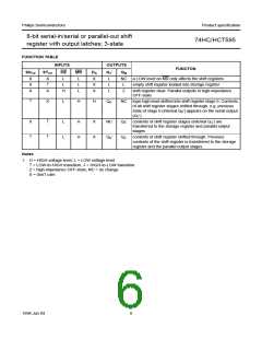
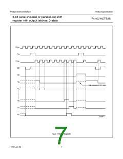
Data is shifted on the positive-going transitions of the
SHCP input. The data in each register is transferred to the
storage register on a positive-going transition of the STCP
input. If both clocks are connected together, the shift
register will always be one clock pulse ahead of the
storage register.
APPLICATIONS
• Serial-to-parallel data conversion
• Remote control holding register.
The shift register has a serial input (DS) and a serial
standard output (Q7’) for cascading. It is also provided with
asynchronous reset (active LOW) for all 8 shift register
stages. The storage register has 8 parallel 3-state bus
driver outputs. Data in the storage register appears at the
output whenever the output enable input (OE) is LOW.
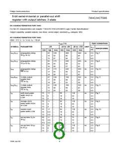
QUICK REFERENCE DATA
GND = 0 V; Tamb = 25 °C; tr = tf = 6 ns.
TYP.
SYMBOL PARAMETER
CONDITIONS
UNIT
HC
HCT
tPHL/tPLH propagation delay
CL = 15 pF; VCC = 5 V
SHCP to Q7’
16
21
ns
STCP to Qn
17
20
ns
MR to Q7’
14
19
ns
fmax
CI
maximum clock frequency SHCP, STCP
input capacitance
100
3.5
115
57
MHz
pF
pF
3.5
130
CPD
power dissipation capacitance per package
notes 1 and 2
Notes
1. CPD is used to determine the dynamic power dissipation (PD in µW):
PD = CPD × VCC2 × fi + ∑ (CL × VCC2 × fo) where:
fi = input frequency in MHz
fo = output frequency in MHz
∑(CL × VCC2 × fo) = sum of outputs
CL = output load capacitance in pF
VCC = supply voltage in V
2. For HC the condition is VI = GND to VCC; for HCT the condition is VI = GND to VCC − 1.5 V.
1998 Jun 04
2

 NXP [ NXP ]