Philips Semiconductors
Product specification
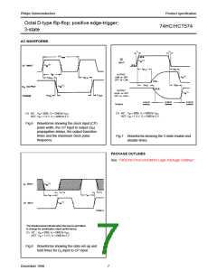
Octal D-type flip-flop; positive
edge-trigger; 3-state
74HC/HCT574
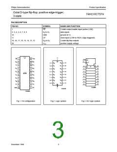
The 8 flip-flops will store the state of
their individual D-inputs that meet the
set-up and hold time requirements on
the LOW-to-HIGH CP transition.
When OE is LOW, the contents of the
8 flip-flops are available at the
outputs.
When OE is HIGH, the outputs go to
the high impedance OFF-state.
Operation of the OE input does not
affect the state of the flip-flops.
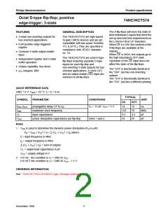
FEATURES
GENERAL DESCRIPTION
• 3-state non-inverting outputs for
bus oriented applications
The 74HC/HCT574 are high-speed
Si-gate CMOS devices and are pin
compatible with low power Schottky
TTL (LSTTL). They are specified in
compliance with JEDEC standard
no. 7A.
• 8-bit positive edge-triggered
register
• Common 3-state output enable
input
The 74HC/HCT574 are octal D-type
flip-flops featuring separate D-type
inputs for each flip-flop and
non-inverting 3-state outputs for bus
oriented applications. A clock (CP)
and an output enable (OE) input are
common to all flip-flops.
• Independent register and 3-state
buffer operation
• Output capability: bus driver
• ICC category: MSI
The “574” is functionally identical to
the “564”, but has non-inverting
outputs.
The “574” is functionally identical to
the “374”, but has a different pinning.
QUICK REFERENCE DATA
GND = 0 V; Tamb = 25 °C; tr = tf = 6 ns
TYPICAL
UNIT
SYMBOL
PARAMETER
CONDITIONS
HC
HCT
tPHL/ tPLH
fmax
propagation delay CP to Qn
maximum clock frequency
input capacitance
CL = 15 pF; VCC = 5 V
14
15
76
3.5
25
ns
123
3.5
22
MHz
pF
CI
CPD
power dissipation capacitance per flip-flop
notes 1 and 2
pF
Notes
1. CPD is used to determine the dynamic power dissipation (PD in µW):
2
PD = CPD × VCC2 × fi + ∑ (CL × VCC × fo) where:
fi = input frequency in MHz
fo = output frequency in MHz
∑ (CL × VCC2 × fo) = sum of outputs
CL = output load capacitance in pF
VCC = supply voltage in V
2. For HC the condition is VI = GND to VCC
For HCT the condition is VI = GND to VCC − 1.5 V
ORDERING INFORMATION
See “74HC/HCT/HCU/HCMOS Logic Package Information”.
December 1990
2

 NXP [ NXP ]