Philips Semiconductors
Product specification
8-bit parallel-in/serial-out shift register
74HC/HCT165
AC WAVEFORMS
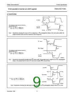
The changing to output assumes internal Q6
opposite state from Q7.
(1) HC : VM = 50%; VI = GND to VCC
.
HCT: VM = 1.3 V; VI = GND to 3 V.
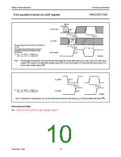
Fig.6 Waveforms showing the clock (CP) to output (Q7 or Q7) propagation delays, the clock pulse width, the
output transition times and the maximum clock frequency.
The changing to output assumes internal Q6
opposite state from Q7.
(1) HC : VM = 50%; VI = GND to VCC
.
HCT: VM = 1.3 V; VI = GND to 3 V.
Fig.7 Waveforms showing the parallel load (PL) pulse width, the parallel load to output (Q7 or Q7) propagation
delays, the parallel load to clock (CP) and clock enable (CE) removal time.
(1) HC : VM = 50%; VI = GND to VCC
.
HCT: VM = 1.3 V; VI = GND to 3 V.
Fig.8 Waveforms showing the data input (Dn) to output (Q7 or Q7) propagation delays when PL is LOW.
December 1990
9

 NXP [ NXP ]