Philips Semiconductors
Product specification
8-bit serial-in/parallel-out shift register
74HC/HCT164
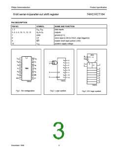
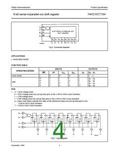
Data is entered serially through one of two inputs (Dsa or
Dsb); either input can be used as an active HIGH enable for
data entry through the other input.
Both inputs must be connected together or an unused
input must be tied HIGH.
FEATURES
• Gated serial data inputs
• Asynchronous master reset
• Output capability: standard
• ICC category: MSI
Data shifts one place to the right on each LOW-to-HIGH
transition of the clock (CP) input and enters into Q0, which
is the logical AND of the two data inputs (Dsa,Dsb) that
existed one set-up time prior to the rising clock edge.
GENERAL DESCRIPTION
The 74HC/HCT164 are high-speed Si-gate CMOS devices
and are pin compatible with low power Schottky TTL
(LSTTL). They are specified in compliance with JEDEC
standard no. 7A.
A LOW level on the master reset (MR) input overrides all
other inputs and clears the register asynchronously,
forcing all outputs LOW.
The 74HC/HCT164 are 8-bit edge-triggered shift registers
with serial data entry and an output from each of the eight
stages.
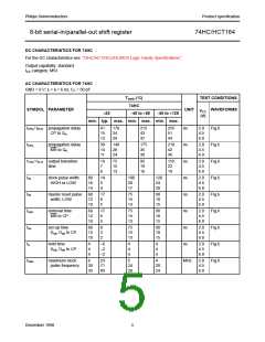
QUICK REFERENCE DATA
GND = 0 V; Tamb = 25 °C; tr = tf = 6 ns
TYPICAL
SYMBOL
tPHL/ tPLH
PARAMETER
propagation delay
CONDITIONS
UNIT
HC
HCT
CL = 15 pF; VCC = 5 V
CP to Qn
MR to Qn
12
11
14
16
ns
ns
fmax
CI
maximum clock frequency
input capacitance
78
61
MHz
pF
3.5
3.5
CPD
power dissipation capacitance per
package
notes 1 and 2
40
40
pF
Notes
1. CPD is used to determine the dynamic power dissipation (PD in µW):
PD = CPD × VCC2 × fi + ∑ (CL × VCC2 × fo) where:
fi = input frequency in MHz
fo = output frequency in MHz
∑ (CL × VCC2 × fo) = sum of outputs
CL = output load capacitance in pF
VCC = supply voltage in V
2. For HC the condition is VI = GND to VCC
For HCT the condition is VI = GND to VCC − 1.5 V
ORDERING INFORMATION
See “74HC/HCT/HCU/HCMOS Logic Package Information”.
December 1990
2

 NXP [ NXP ]