Philips Semiconductors
Product specification
Quad buffer/line driver; 3-state
74AHC125; 74AHCT125
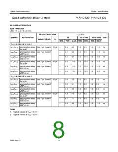
Type 74AHCT125
GND = 0 V; tr = tf ≤ 3.0 ns.
TEST CONDITIONS
WAVEFORMS CL
Tamb (°C)
SYMBOL
PARAMETER
25
−40 to +85 −40 to +125 UNIT
MIN. TYP. MAX. MIN. MAX. MIN. MAX.
VCC = 4.5 to 5.5 V; note 1
tPHL/tPLH propagation delay see Figs 5 and 7 15 pF
nA to nY
−
−
−
−
−
−
3.0
3.4
4.5
4.3
4.9
6.5
5.5
5.1
6.8
7.5
7.3
8.8
1.0
1.0
1.0
1.0
1.0
1.0
6.5
6.0
8.0
8.5
8.3
10.0
1.0
1.0
1.0
1.0
1.0
1.0
7.0
6.5
8.5
9.5
9.5
11.0
ns
ns
ns
ns
ns
ns
tPZH/tPZL propagation delay see Figs 6 and 7
nOE to nY
tPHZ/tPLZ propagation delay
nOE to nY
tPHL/tPLH propagation delay see Figs 5 and 7 50 pF
nA to nY
tPZH/tPZL propagation delay see Figs 6 and 7
nOE to nY
tPHZ/tPLZ propagation delay
nOE to nY
Note
1. Typical values at VCC = 5.0 V.
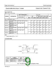
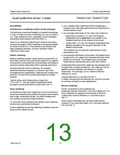
AC WAVEFORMS
V
handbook, halfpage
I
(1)
V
nA INPUT
M
GND
t
t
PHL
PLH
V
OH
(1)
V
nY OUTPUT
M
V
MNA230
OL
(1)
(1)
VI INPUT
REQUIREMENTS
VM
VM
OUTPUT
FAMILY
INPUT
AHC
GND to VCC
50% VCC 50% VCC
1.5 V 50% VCC
AHCT
GND to 3.0 V
Fig.5 The input (nA) to output (nY) propagation delays.
9
1999 Sep 27

 NXP [ NXP ]