Philips Semiconductors
Product specification
Quad buffer/line driver; 3-state
74AHC125; 74AHCT125
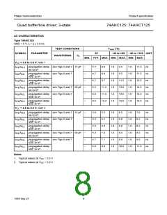
RECOMMENDED OPERATING CONDITIONS
74AHC
74AHCT
SYMBOL
PARAMETER
DC supply voltage
CONDITIONS
UNIT
MIN. TYP. MAX. MIN. TYP. MAX.
VCC
VI
2.0
0
5.0
−
5.5
4.5
0
5.0
−
5.5
V
input voltage
5.5
5.5
V
VO
output voltage
0
−
VCC
+85
0
−
VCC
+85
V
Tamb
operating ambient temperature
range
see DC and AC
characteristics per
device
−40
−40
+25
+25
−40
+25
+25
°C
+125 −40
+125 °C
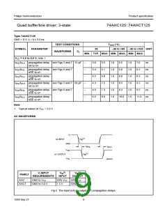
tr,tf (∆t/∆f) input rise and fall rates
VCC = 3.3 V ±0.3 V
VCC = 5 V ±0.5 V
−
−
−
−
100
20
−
−
−
−
−
ns/V
20
LIMITING VALUES
In accordance with the Absolute Maximum Rating System (IEC 134); voltages are referenced to GND (ground = 0 V).
SYMBOL
PARAMETER
DC supply voltage
CONDITIONS
MIN. MAX. UNIT
VCC
VI
−0.5 +7.0
−0.5 +7.0
V
input voltage range
V
IIK
DC input diode current
DC output diode current
VI < −0.5 V; note 1
VO < −0.5 V or VO > VCC + 0.5 V; note 1
−
−20
±20
±25
±75
mA
mA
mA
mA
IOK
IO
−
DC output source or sink current −0.5 V < VO < VCC + 0.5 V
DC VCC or GND current
−
ICC
Tstg
PD
−
storage temperature range
−65
−
+150 °C
500 mW
power dissipation per package
for temperature range: −40 to +125 °C; note 2
Notes
1. The input and output voltage ratings may be exceeded if the input and output current ratings are observed.
2. For SO packages: above 70 °C the value of PD derates linearly with 8 mW/K.
For TSSOP packages: above 60 °C the value of PD derates linearly with 5.5 mW/K.
1999 Sep 27
5

 NXP [ NXP ]