Philips Semiconductors
Product specification
Quad buffer/line driver; 3-state
74AHC125; 74AHCT125
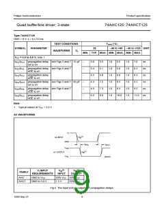
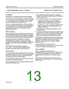
V
handbook, full pagewidth
I
(1)
t
V
nOE INPUT
M
GND
t
PLZ
PZL
V
CC
OUTPUT
LOW-to-OFF
OFF-to-LOW
(1)
V
M
V
+0.3 V
V
OL
V
OL
t
t
PHZ
PZH
V
OH
−0.3 V
OH
OUTPUT
(1)
V
HIGH-to-OFF
OFF-to-HIGH
M
GND
outputs
enabled
outputs
enabled
outputs
disabled
MNA231
(1)
(1)
VI INPUT
REQUIREMENTS
VM
VM
OUTPUT
FAMILY
INPUT
AHC
GND to VCC
50% VCC 50% VCC
1.5 V 50% VCC
AHCT
GND to 3.0 V
Fig.6 The 3-state enable and disable times.
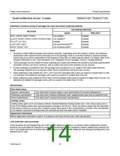
S1
handbook, full pagewidth
V
CC
open
V
CC
GND
R
=
L
1000 Ω
V
V
O
I
PULSE
D.U.T.
GENERATOR
C
R
L
T
MNA232
TEST
S1
tPLH/tPHL
tPLZ/tPZL
tPHZ/tPZH
open
VCC
GND
Fig.7 Load circuitry for switching times.
10
1999 Sep 27

 NXP [ NXP ]