Philips Semiconductors
Product specification
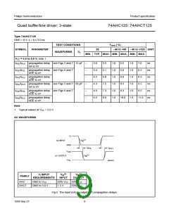
Quad buffer/line driver; 3-state
74AHC125; 74AHCT125
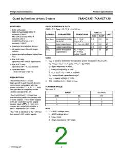
FEATURES
QUICK REFERENCE DATA
GND = 0 V; Tamb = 25 °C; tr = tf ≤ 3.0 ns.
• ESD protection:
HBM EIA/JESD22-A114-A
exceeds 2000 V
MM EIA/JESD22-A115-A
exceeds 200 V
CDM EIA/JESD22-C101
exceeds 1000 V
TYPICAL
SYMBOL
PARAMETER
CONDITIONS
UNIT
ns
AHC AHCT
tPHL/tPLH propagation delay CL = 15 pF;
nA to nY VCC = 5 V
input capacitance VI = VCC or GND 3.0
3.0
3.0
CI
3.0
4.0
12
pF
pF
pF
• Balanced propagation delays
CO
CPD
output capacitance
4.0
10
• All inputs have Schmitt-trigger
actions
power dissipation
capacitance
CL = 50 pF;
f = 1 MHz;
notes 1 and 2
• Inputs accepts voltages higher than
VCC
Notes
• For AHC only:
1. CPD is used to determine the dynamic power dissipation (PD in µW).
PD = CPD × VCC2 × fi + ∑ (CL × VCC2 × fo) where:
fi = input frequency in MHz;
operates with CMOS input levels
• For AHCT only:
operates with TTL input levels
fo = output frequency in MHz;
• Specified from
−40 to +85 and +125 °C.
∑ (CL × VCC2 × fo) = sum of outputs;
CL = output load capacitance in pF;
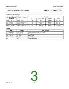
DESCRIPTION
VCC = supply voltage in Volts.
The 74AHC/AHCT125 are
2. The condition is VI = GND to VCC
.
high-speed Si-gate CMOS devices
and are pin compatible with low
power Schottky TTL (LSTTL). They
are specified in compliance with
JEDEC standard No. 7A.
FUNCTION TABLE
See note 1.
INPUT
nOE
OUTPUT
nY
The 74AHC/AHCT125 are four
non-inverting buffer/line drivers with
3-state outputs. The 3-state outputs
(nY) are controlled by the output
enable input (nOE). A HIGH at n
causes the outputs to assume a
HIGH-impedance OFF-state.
nA
L
L
L
H
X
L
H
Z
H
Note
1. H = HIGH voltage level;
L = LOW voltage level;
X = don’t care;
The ‘125’ is identical to the ‘126’ but
has active LOW enable inputs.
Z = high-impedance OFF-state.
1999 Sep 27
2

 NXP [ NXP ]