Subject
Metal Film(Thin Film) Chip Resistors PRODUCT SPECIFICATION FOR INFORMATION
Part No.
Spec. No.
151-SRA-E102R
E R A 3
10 8
-
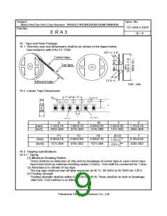
14. Tape and Reel Package
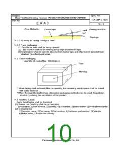
14.1 Structure and reel dimensions shall be as shown in the figure below.
Inaccordance with EIAJ ET-7200.
9.0 +/- 1.0
Carrier tape
Top tape
11.4 +/-
Adhesive tape
Unit : mm
14.2 Carrier Tape Dimensions
P1
P2
P0
Do
Sprocket hole
E
F
W
B
A
Chip resistor
T
Chip hole
A
B
W
F
E
(mm)
(inch)
1.10±0.10
.043±.004
1.90±0.10
.074±.004
8.00±0.20
.314±.008
3.50±0.05
.137±.002
1.75±0.10
.069±.004
P1
4.00±0.10
P2
2.00±0.05
P0
4.00±0.10
D0
1.50 ±00.10
T
(mm)
0.70±0.05
.059 ±.0004
(inchi)
.157±.004
.079±.002
.157±.004
.028±.002
14.3 Tapping specifications
14.3.1 Taping
(1) Minimum Bending Radius
There shall be no defection of chip and no breakage of carrier tape in case carrier tape
have been bent by minimum bending radius (15mm). Test shall be conducted for 1 time.
(2) Resistance to climate of top tape
The top tape shall not tear off after exposure at 60 oC, 90 %RH to 95 %RH for 120 h.
(3) Peeling strength
Peeling strength shall be within 0.049 N to 0.49 N. There shall be no burr or breakage
after test. Test method is as follows:
Panasonic Electronic Devices Co., Ltd.

 PANASONIC [ PANASONIC ]