Subject
Metal Film(Thin Film) Chip Resistors PRODUCT SPECIFICATION FOR INFORMATION
Part No.
Spec. No.
151-SRA-E102R
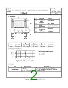
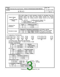
E R A 3
10 3
-
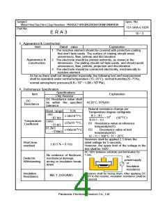
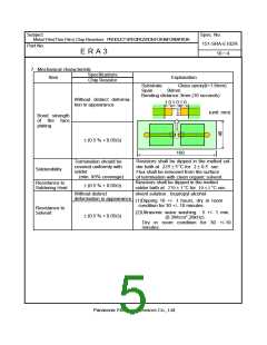
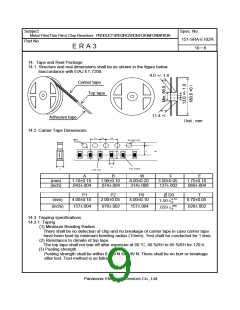
5. Appearance & Construction
Item
Rated value
Explanation
1. The resistive element should be covered with protective coating
that don’t fade easily. The surface of coating should avoid
unevenness, flaw, pinhole and discoloration.
Appearance &
Construction
2. The electrode should be printed uniformly, as shown in the
dimensions. The plating should not fade easily, and should avoid
unevenness, flaw, pinhole, projection and discoloration.
3. The electrode should be connected electrically, mechanically to
resistive element.
As far as there shall not designation especially, the following test and measurement
shall be operated under normal temperature (15~35°C), normal humidity(25~75%),
normal atmospheric pressure(8.6×10⁴ ~1.06×10⁵ Pa ).
6. Performance Specification
Specifications
Chip Resistor
Item
Explanation
DC Resistance value shall
be within the specified
tolerance
DC
Resistance
At 20°C, 65%RH
Natural resistance change per
Temperature degree centigrade.
R 2 − R1
R1(t 2 − t1)
R1 : Resistance value at reference
temperature(t1)
Resit. range
10Ω
~97.6Ω
100Ω
~33 kΩ
33.2kΩ
~330kΩ
TCR
± 50x10-6/°C
×106
(10-6/℃)
Temperature
Coefficient
±25x10 -6/°C
±100x10-6/°C
R2
: Resistance value at test
temperature(t2)
t2 – t1 = 100°C t1 = 25°C
Resistors shall be applied 2.5 times the
rated voltage for 5 seconds.
However, the upper limit of the voltage in the
test shall be 150V.
Short-time
overload
± (0.5 % + 0.1Ω)
AC 100V between substrate and termination for
1 min.
No evidence of flashover,
mechanical damage,
arcing or insulation break-
down
AC
Dielectric
Withstanding
powersupply
or
Insulation
resistance
Insulation
Resistance
Resistors shall be facing down. After applying DC
100V to the resistor, insulation resistance shall be
measured.
Min.1,000M
Ω
Panasonic Electronic Devices Co., Ltd.

 PANASONIC [ PANASONIC ]