NVMTS4D3N15MC
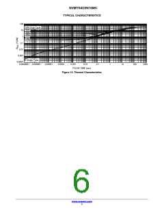
THERMAL RESISTANCE RATINGS
Symbol
Parameter
Max
0.5
Unit
Junction−to−Case – Steady State (Note 2)
Junction−to−Ambient – Steady State (Note 2)
°C/W
R
q
JC
JA
R
31.4
q
ELECTRICAL CHARACTERISTICS (T = 25°C unless otherwise noted)
J
Symbol
Parameter
Test Condition
Min
Typ
Max
Unit
OFF CHARACTERISTICS
V
Drain−to−Source Breakdown Voltage
V
= 0 V, I = 250 mA
150
−
−
−
V
(BR)DSS
GS
D
V
/ T
Drain−to−Source Breakdown Voltage
Temperature Coefficient
I = 250 mA, ref to 25°C
D
−
49.84
mV/°C
(BR)DSS
J
I
Zero Gate Voltage Drain Current
V
V
= 0 V,
T = 25°C
−
−
−
−
−
−
1
mA
mA
nA
DSS
GS
DS
J
= 120 V
T = 125°C
J
10
100
I
Gate−to−Source Leakage Current
V
= 0 V, V =
GS
20 V
GSS
DS
GS
ON CHARACTERISTICS (Note 3)
V
Gate Threshold Voltage
V
= V , I = 521 mA
2.5
−
3.6
−9.93
3.4
4.5
−
V
GS(TH)
DS
D
V
/ T
J
Negative Threshold Temperature Coefficient
Drain−to−Source On Resistance
I = 250 mA, ref to 25°C
D
mV/°C
mW
GS(TH)
R
V
GS
= 10 V, I = 95 A
−
4.45
DS(on)
D
g
Forward Transconductance
V
= 5 V, I = 95 A
−
−
177
1.1
−
−
S
FS
DS
D
R
Gate−Resistance
T = 25°C
A
W
G
CHARGES & CAPACITANCES
C
Input Capacitance
V
V
= 0 V, f = 1 MHz,
= 75V
−
−
−
−
−
−
−
−
6514
1750
12.5
79
−
−
−
−
−
−
−
−
pF
nC
ISS
GS
DS
C
Output Capacitance
Reverse Transfer Capacitance
Total Gate Charge
OSS
RSS
C
Q
V
D
= 10 V, V = 75 V,
DS
= 95 A
G(TOT)
GS
I
Q
Threshold Gate Charge
Gate−to−Source Charge
Gate−to−Drain Charge
Plateau Voltage
21
G(TH)
V
D
= 10 V, V = 75 V,
GS
DS
I
= 95 A
Q
36
GS
GD
GP
Q
V
11
5.8
SWITCHING CHARACTERISTICS, V = 10 V (Note 3)
GS
t
Turn−On Delay Time
Rise Time
V
D
= 10 V, V =75 V,
−
−
−
−
38
11
48
8
−
−
−
−
ns
d(ON)
GS
DS
I
= 95 A, R = 6 W
G
t
r
t
Turn−Off Delay Time
Fall Time
d(OFF)
t
f
DRAIN−SOURCE DIODE CHARACTERISTICS
V
Forward Diode Voltage
V
S
= 0 V,
T = 25°C
−
−
−
−
−
−
0.86
0.80
85
1.2
−
V
SD
GS
J
I
= 95 A
T = 125°C
J
t
Reverse Recovery Time
Charge Time
V
S
= 0 V, dI /dt = 100 A/ms,
= 95 A
−
ns
RR
GS
S
I
t
t
58
−
a
Discharge Time
38
−
b
Q
Reverse Recovery Charge
194
nC
RR
−
Product parametric performance is indicated in the Electrical Characteristics for the listed test conditions, unless otherwise noted. Product
performance may not be indicated by the Electrical Characteristics if operated under different conditions.
3. Switching characteristics are independent of operating junction temperatures
www.onsemi.com
2

 ONSEMI [ ONSEMI ]