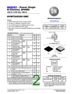
MOSFET – Power, Single
N-Channel, DFNW8
150 V, 4.45 mW, 165 A
NVMTS4D3N15MC
Features
www.onsemi.com
• Small Footprint (8x8 mm) for Compact Design
• Low R
to Minimize Conduction Losses
DS(on)
• Low Q and Capacitance to Minimize Driver Losses
G
V
R
MAX
I MAX
D
(BR)DSS
DS(ON)
• AEC−Q101 Qualified and PPAP Capable
• These Devices are Pb−Free, Halogen Free/BFR Free and are RoHS
Compliant
150 V
4.45 mW @ 10 V
165 A
D (5, 6, 7, 8)
MAXIMUM RATINGS (T = 25°C unless otherwise noted)
J
Symbol
Parameter
Drain−to−Source Voltage
Value
150
20
Unit
V
V
DSS
G (1)
V
GS
Gate−to−Source Voltage
V
I
Continuous Drain
Steady
State
T
T
= 25°C
165
A
D
C
Current R
(Note 2)
S (2, 3, 4)
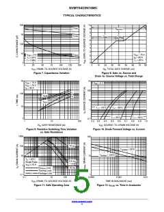
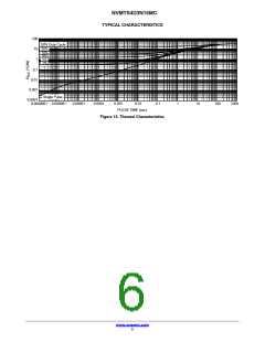
N−CHANNEL MOSFET
q
JC
P
Power Dissipation
(Note 2)
292
117
146
21
W
A
D
R
q
JC
I
D
Continuous Drain
Current R (Note 2)
Steady
State
=
C
100°C
q
JC
P
Power Dissipation
(Note 2)
W
A
D
R
q
JC
I
D
Continuous Drain
Current R
Steady
State
T = 25°C
A
Top
Bottom
q
JA
(Notes 1, 2)
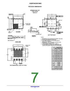
DFNW8
CASE 507AP
P
I
Power Dissipation
5
W
A
D
R
(Notes 1, 2)
q
JA
Continuous Drain
Current R
Steady
State
T =
15
MARKING DIAGRAM
D
A
100°C
q
JA
(Notes 1, 2)
4D3N15MC
AWLYWW
P
D
Power Dissipation
2.4
W
R
(Notes 1, 2)
q
JA
I
Pulsed Drain Current
T = 25°C, t = 10 ms
900
A
DM
A
p
4D3N15MC = Specific Device Code
A
WL
Y
= Assembly Location
= Wafer Lot Code
= Year Code
T , T
Operating Junction and Storage Temperature
Range
−55 to
°C
J
stg
+175
I
S
Source Current (Body Diode)
243
A
WW
= Work Week Code
E
AS
Single Pulse Drain−to−Source Avalanche
3390
mJ
Energy (I = 14.1 A)
L
ORDERING INFORMATION
T
L
Lead Temperature Soldering Reflow for
Soldering Purposes (1/8″ from case for 10 s)
260
°C
†
Device
Package
Shipping
Stresses exceeding those listed in the Maximum Ratings table may damage the
device. If any of these limits are exceeded, device functionality should not be
assumed, damage may occur and reliability may be affected.
NVMTS4D3N15MC
DFNW8
(Pb−Free)
3000 / Tape &
Reel
2
1. Surface−mounted on FR4 board using 1 in pad size, 1 oz Cu pad.
†For information on tape and reel specifications,
including part orientation and tape sizes, please
refer to our Tape and Reel Packaging Specifications
Brochure, BRD8011/D.
2. The entire application environment impacts the thermal resistance values shown,
they are not constants and are only valid for the particular conditions noted
© Semiconductor Components Industries, LLC, 2020
1
Publication Order Number:
December, 2020 − Rev. 0
NVMTS4D3N15MC/D

 ONSEMI [ ONSEMI ]