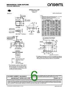
MECHANICAL CASE OUTLINE
PACKAGE DIMENSIONS
WDFN8 3.3x3.3, 0.65P
CASE 511AB
1
SCALE 2:1
2X
ISSUE D
DATE 23 APR 2012
NOTES:
0.20
C
1. DIMENSIONING AND TOLERANCING PER ASME Y14.5M, 1994.
2. CONTROLLING DIMENSION: MILLIMETERS.
3. DIMENSION D1 AND E1 DO NOT INCLUDE MOLD FLASH
PROTRUSIONS OR GATE BURRS.
D
A
B
E
2X
D1
MILLIMETERS
INCHES
NOM
0.030
−−−
0.012
0.20
C
8
1
7
6
5
4
DIM
A
A1
b
c
MIN
0.70
0.00
0.23
0.15
NOM
0.75
−−−
0.30
0.20
MAX
MIN
MAX
0.031
0.002
0.016
0.010
0.80
0.05
0.40
0.25
0.028
0.000
0.009
0.006
4X
q
E1
0.008
D
3.30 BSC
3.05
2.11
3.30 BSC
3.05
1.60
0.30
0.65 BSC
0.41
0.80
0.43
0.130 BSC
0.120
0.083
0.130 BSC
0.120
0.063
0.012
0.026 BSC
0.016
0.032
0.017
0.005
0.059
−−−
D1
D2
E
E1
E2
E3
e
G
K
L
L1
M
2.95
1.98
3.15
2.24
0.116
0.078
0.124
0.088
c
2
3
A1
TOP VIEW
2.95
1.47
0.23
3.15
1.73
0.40
0.116
0.058
0.009
0.124
0.068
0.016
0.10
0.10
C
C
A
C
6X
e
0.012
0.026
0.012
0.002
0.055
0
0.020
0.037
0.022
0.008
0.063
0.30
0.65
0.30
0.06
1.40
0
0.51
0.95
0.56
0.20
1.60
SEATING
PLANE
0.13
1.50
−−−
DETAIL A
SIDE VIEW
DETAIL A
q
12
12
_
_
_
_
8X b
0.10
0.05
C
C
A
B
SOLDERING FOOTPRINT*
8X
e/2
0.42
0.65
4X
L
4X
0.66
PITCH
1
8
4
5
PACKAGE
OUTLINE
K
E2
M
E3
3.60
L1
D2
G
2.30
BOTTOM VIEW
0.57
0.47
0.75
GENERIC
MARKING DIAGRAM*
2.37
3.46
1
XXXXX
DIMENSION: MILLIMETERS
AYWWG
*For additional information on our Pb−Free strategy and soldering
details, please download the ON Semiconductor Soldering and
Mounting Techniques Reference Manual, SOLDERRM/D.
G
XXXXX = Specific Device Code
A
Y
= Assembly Location
= Year
WW
G
= Work Week
= Pb−Free Package
*This information is generic. Please refer to
device data sheet for actual part marking.
Pb−Free indicator, “G” or microdot “G”, may
or may not be present. Some products may
not follow the Generic Marking.
Electronic versions are uncontrolled except when accessed directly from the Document Repository.
Printed versions are uncontrolled except when stamped “CONTROLLED COPY” in red.
DOCUMENT NUMBER:
DESCRIPTION:
98AON30561E
WDFN8 3.3X3.3, 0.65P
PAGE 1 OF 1
onsemi and
are trademarks of Semiconductor Components Industries, LLC dba onsemi or its subsidiaries in the United States and/or other countries. onsemi reserves
the right to make changes without further notice to any products herein. onsemi makes no warranty, representation or guarantee regarding the suitability of its products for any particular
purpose, nor does onsemi assume any liability arising out of the application or use of any product or circuit, and specifically disclaims any and all liability, including without limitation
special, consequential or incidental damages. onsemi does not convey any license under its patent rights nor the rights of others.
© Semiconductor Components Industries, LLC, 2019
www.onsemi.com

 ONSEMI [ ONSEMI ]