NL7WB66
ADDITIONAL APPLICATIONS CHARACTERISTICS (Voltage Reference to GND Unless Noted)
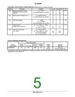
Symbol
Parameter
Condition
V
CC
(V)
Typical 255C
Unit
BW
Maximum On−Channel −3.0 dB
Bandwidth or Minimum Frequency
Response
V
IS
= 0 dBm
2.0
3.0
4.5
102
180
186
MHz
V
V
centered between V and GND
IS
CC
V
ONL
Maximum Feed−Through On Loss
V
= 0 dBm @ 10 kHz
centered between V and GND
2.0
3.0
4.5
−2.2
−0.8
−0.4
dB
dB
pC
%
IS
IS
CC
V
ISO
Off−Channel Isolation
f = 100 kHz
2.0
3.0
4.5
−73
−74
−75
V
= 1.0 V RMS
IS
V
IS
centered between V and GND
CC
Q
Charge Injection
Enable Input to Common I/O
V
= V to GND, F = 20 kHz
IS CC IS
t = t = 3.0 nS
3.0
5.5
4.8
7.5
r
f
R
= 0 ꢀ, C = 100 pF
IS
L
THD
Total Harmonic Distortion
TDH + Noise
F
IS
= 10 Hz to 100 kHz,
= 600 ꢀ, C = 50 pF
= 3.0 V Sine Wave
PP
R = R
3.0
5.5
0.19
0.06
L
gen
L
V
IS
V
IS
= 5.0 V Sine Wave
PP
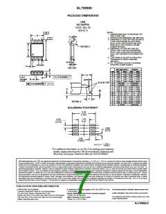
DEVICE ORDERING INFORMATION
Device Nomenclature
Circuit
Indicator
Device
Function
Package
Suffix
Device
Order Number
Package
Type
Tape and
Reel Size
Technology
NL7WB66USG
NL
AS
2066
US
US8
(Pb−Free)
178 mm (7″)
3000 Units / Tape & Reel
†For information on tape and reel specifications, including part orientation and tape sizes, please refer to our Tape and Reel Packaging
Specifications Brochure, BRD8011/D.
http://onsemi.com
5

 ONSEMI [ ONSEMI ]