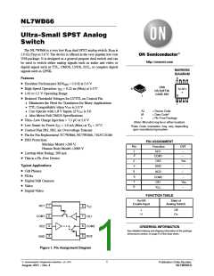
NL7WB66
MAXIMUM RATINGS
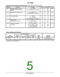
Symbol
Rating
Value
*0.5 to )7.0
*0.5 to )7.0
*0.5 to )7.0
*50
Unit
V
V
CC
DC Supply Voltage
V
DC Input Voltage
V
I
O
V
DC Output Voltage
V
I
DC Input Diode Current
DC Output Diode Current
DC Output Sink Current
DC Supply Current per Supply Pin
DC Ground Current per Ground Pin
Storage Temperature Range
V < GND
mA
mA
mA
mA
mA
°C
IK
I
I
V
< GND
O
*50
OK
I
$50
O
I
$100
CC
I
$100
GND
T
*65 to )150
260
STG
T
Lead Temperature, 1 mm from Case for 10 Seconds
Junction Temperature under Bias
Thermal Resistance
°C
L
T
)150
°C
J
ꢁ
250
°C/W
mW
−
JA
P
Power Dissipation in Still Air at 85°C
Moisture Sensitivity
250
D
MSL
Level 1
F
R
Flammability Rating
Oxygen Index: 28 to 34
UL 94 V−0 @ 0.125 in
−
V
ESD
ESD Withstand Voltage
Human Body Model (Note 2)
Machine Model (Note 3)
Charged Device Model (Note 4)
> 2000
> 200
N/A
V
Stresses exceeding Maximum Ratings may damage the device. Maximum Ratings are stress ratings only. Functional operation above the
Recommended Operating Conditions is not implied. Extended exposure to stresses above the Recommended Operating Conditions may affect
device reliability.
1. Measured with minimum pad spacing on an FR4 board, using 10 mm−by−1 inch, 2−ounce copper trace with no air flow.
2. Tested to EIA/JESD22−A114−A.
3. Tested to EIA/JESD22−A115−A.
4. Tested to JESD22−C101−A.
RECOMMENDED OPERATING CONDITIONS
Symbol
Characteristics
Min
1.65
GND
GND
GND
Max
5.5
Unit
V
V
CC
Positive DC Supply Voltage
Digital Input Voltage (Enable)
V
IN
5.5
V
V
IO
Static or Dynamic Voltage Across an Off Switch
Analog Input Voltage
V
V
CC
CC
V
IS
NO
V
V
COM
T
A
Operating Temperature Range, All Package Types
−55
+125
°C
t , t
Input Rise or Fall Time
(Enable Input)
V
V
= 3.3 V + 0.3 V
= 5.0 V + 0.5 V
0
0
100
20
ns/V
r
f
CC
CC
http://onsemi.com
2

 ONSEMI [ ONSEMI ]