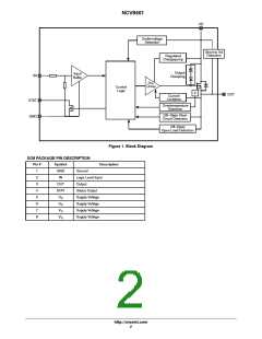
NCV8461
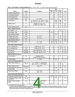
Table 3. ELECTRICAL CHARACTERISTICS (V = 13.5 V; −40°C < T < 150°C unless otherwise specified)
D
J
Value
Typ
−
Min
Max
34
Rating
Symbol
Conditions
Unit
V
Operating Supply Voltage
Undervoltage Shutdown
Undervoltage Restart
Overvoltage Protection
On Resistance
V
D
5
V
5
V
UV
UV_Res
V
5.5
V
V
OV
R
ON
I
D
= 4 mA
41
V
I
= 0.3 A; 6 V < V < 40 V, T = 25°C
250
450
350
700
mW
out
D
J
I
= 0.3 A; 6 V < V < 40 V, T = 150°C
D J
out
Standby Current
I
D
Off State, V = V = 0 V
13
1
35
1.7
mA
mA
in
out
On State; V = 5 V, I = 0 A
in
out
Output Leakage Current
INPUT CHARACTERISTICS
Input Voltage − Low
I
12
mA
L(off)
V
in_low
0.8
V
V
Input Voltage − High
V
in_high
2.2
Input Hysteresis Voltage
Off State Input Current
On State Input Current
Input Resistance (Note 3)
Input Clamp Voltage
V
0.3
3.5
V
hyst
I
V
V
= 0.7 V
1
1
10
10
mA
mA
KW
V
in_OFF
in
I
= 5.0 V
in_ON
in
R
1.5
I
V
in_cl
I
= 1 mA
= −1 mA
14
−18
16
−16
18
−14
in
I
in
SWITCHING CHARACTERISTICS
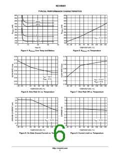
Turn−On Delay Time
Turn−Off Delay Time
Slew Rate On
t
t
to 90% V , R = 47 W
140
170
2
ms
d_on
out
L
to 10% V , R = 47 W
ms
d_off
out
L
dV /dt
out on
10% to 30% Vout, R = 47 W
V / ms
V / ms
L
Slew Rate Off
dV /dt
out off
70% to 40% Vout, R = 47 W
2
L
REVERSE BATTERY (Note 3)
Reverse Battery
−V
Requires a 150 W
32
V
V
D
Resistor in GND Connection
Forward Voltage
V
F
T = 150°C
J
0.6
STATUS PIN CHARACTERISTICS
Status Output Voltage Low
V
I
= 1.6 mA, T = −40°C to 25°C
0.4
0.6
V
stat_low
stat
J
I
= 1.6 mA, T = 150°C (Note 3)
J
stat
Status Leakage Current
I
V
stat
= 5 V
10
mA
ms
stat_leakage
Status Invalid Time After Posit-
ive Input Slope
T
300
700
d(STAT)
Status Clamp Voltage
V
stat_cl
I
= 1 mA
= −1 mA
10
−1.4
V
stat
stat
I
PROTECTION FUNCTIONS (Note 4)
Temperature Shutdown (Note 3)
T
150
0.7
175
10
200
2
°C
°C
SD
T
SD_hyst
Temperature Shutdown Hyster-
esis (Note 3)
Output Current Limit Initial
Peak
I
lim
T = −40°C, V = 20 V (Note 3)
A
J
D
T = 25°C
1.2
J
T = 150°C (Note 3)
J
3. Not subjected to production testing
4. To ensure long term reliability under heavy overload or short circuit conditions, protection and related diagnostic signals must be used
together with a proper hardware/software strategy. If the devices operates under abnormal conditions this hardware/software solutions
must limit the duration and number of activation cycles.
http://onsemi.com
4

 ONSEMI [ ONSEMI ]