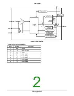
NCV8461
Table 1. MAXIMUM RATINGS
Value
Min
Max
40
Rating
DC Supply Voltage (Note 1)
Symbol
Unit
V
V
D
−16
Peak Transient Input Voltage (Note 1)
V
peak
60
V
(Load Dump XX V, V = 14 V, ISO7637−2 pulse5)
D
Input Voltage
V
−10
−5
−
16
V
mA
A
in
Input Current
I
in
5
Output Current (Note 1)
Status Current
I
Internally Limited
5
out
I
−5
mA
W
status
Power Dissipation Tc = 25°C (Note 1)
Electrostatic Discharge (Note 1)
P
tot
1.5
DC
(HBM Model 100 pF / 1500 W)
Input
4
4
5
5
kV
kV
kV
kV
Status
Output
V
D
Single Pulse Inductive Load Switching Energy (Note 1)
= 13.5 V; I = 0.5 A, T = 150°C
E
AS
−
300
mJ
V
D
L
Jstart
Operating Junction Temperature
Storage Temperature
T
−40
−55
+150
+150
°C
°C
J
T
storage
Stresses exceeding Maximum Ratings may damage the device. Maximum Ratings are stress ratings only. Functional operation above the
Recommended Operating Conditions is not implied. Extended exposure to stresses above the Recommended Operating Conditions may affect
device reliability.
1. Not subjected to production testing
Table 2. THERMAL RESISTANCE RATINGS
Parameter
Symbol
Max. Value
Units
Thermal Resistance (Note 2)
°C/W
Junction−to−Lead
R
31
84
thJL
thJA
Junction−to−Ambient (6 cm square pad size, FR−4, 2 oz Cu)
R
2. Reverse Output current has to be limited by the load to stay within absolute maximum ratings and thermal performance.
http://onsemi.com
3

 ONSEMI [ ONSEMI ]