NCV7703
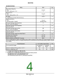
MAXIMUM RATINGS
Rating
Value
Unit
Power Supply Voltage (V )
V
S
(DC)
−0.3 to 40
−1
(AC), t < 500 ms, Ivs > −2 A
Output Pin OUTx
(DC)
(AC), t < 500 ms, IOUTx > −2 A
V
−0.3 to 40
−1
Pin Voltage
(Logic Input pins, SI, SCLK, CSB, SO, EN, V
−0.3 to 7
V
A
)
CC
Output Current (OUTx)
(DC)
−1.8 to 1.8
(AC) (50 ms pulse, 1 s period)
Internally Limited
Electrostatic Discharge, Human Body Model,
V , OUT1, OUT2, OUT3 (Note 3)
S
6
kV
kV
V
Electrostatic Discharge, Human Body Model,
all other pins (Note 3)
2
Electrostatic Discharge, Machine Model,
V , OUT1, OUT2, OUT3 (Note 3)
S
300
200
Electrostatic Discharge, Machine Model,
all other pins (Note 3)
V
Electrostatic Discharge, Charge Device Model (Note 3)
Operating Junction Temperature
1
kV
°C
°C
−
−40 to 150
−55 to 150
MSL3
Storage Temperature Range
Moisture Sensitivity Level (MAX 260°C Processing)
Stresses exceeding Maximum Ratings may damage the device. Maximum Ratings are stress ratings only. Functional operation above the
Recommended Operating Conditions is not implied. Extended exposure to stresses above the Recommended Operating Conditions may affect
device reliability.
Thermal Parameters
Test Conditions (Typical Value)
Unit
14 Pin Fused SOIC Package
min−pad board
1″ pad board
(Note 1)
(Note 2)
Junction−to−Lead (psi−JL8, Y ) or Pins 1, 7, 8, 14
23
22
83
°C/W
°C/W
JL8
Junction−to−Ambient (R , q
)
122
q
JA JA
2
1. 1−oz copper, 67 mm copper area, 0.062″ thick FR4.
2
2. 1−oz copper, 645 mm copper area, 0.062″ thick FR4.
3. This device series incorporates ESD protection and is tested by the following methods:
ESD HBM tested per AEC−Q100−002 (EIA/JESD22−A114)
ESD MM tested per AEC−Q100−003 (EIA/JESD22−A115)
ESD CDM tested per EIA/JES D22/C101, Field Induced Charge Model
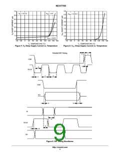
http://onsemi.com
4

 ONSEMI [ ONSEMI ]