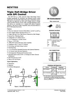
NCV7703
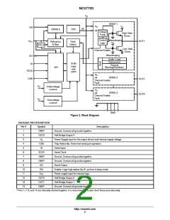
V
S
DRIVE 1
V
S
V
S
EN
clk
ENABLE
OSC
clk
Charge
Pump
High−Side
Driver
Control
Logic
Waveshaping
V
CC
OUT1
Reference
& Bias
Fault
Detect
V
S
UVLO
Low−Side
Driver
Channel Enable
Waveshaping
SO
Under−Load
Overcurrent
Thermal
16 Bit
Logic
and
SI
Warning/Shutdown
SPI
SCLK
Latch
V
S
clk
DRIVE 2
Channel Enable
Fault
CSB
OUT2
OUT3
V
Undervoltage
Lockout
S
V
S
DRIVE 3
Channel Enable
Fault
clk
V
S
Overvoltage
Lockout
GND
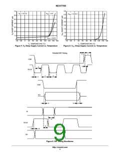
Figure 2. Block Diagram
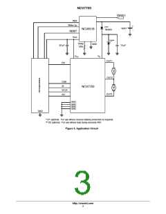
PACKAGE PIN DESCRIPTION
Pin #
1
Symbol
GND*
Description
Ground. Connect all grounds together.
Half Bridge Output 3.
2
OUT3
3
V
Power Supply input for the output drivers and internal supply voltage.
Chip Select Bar. Active low serial port operation.
Serial Input
S
4
CSB
SI
5
6
SCLK
GND*
GND*
SO
Serial Clock
7
Ground. Connect all grounds together.
Ground. Connect all grounds together.
Serial Output
8
9
10
11
12
13
14
EN
Enable. Logic high wakes the IC up from a sleep mode.
Power supply input for internal logic.
Half Bridge Output 2.
V
CC
OUT2
OUT1
GND*
Half Bridge Output 1.
Ground. Connect all grounds together.
* Pins 1, 7, 8, and 14 are internally shorted together. It is recommended to also short these pins externally.
http://onsemi.com
2

 ONSEMI [ ONSEMI ]