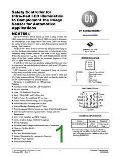
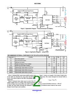
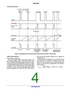
NCV7694
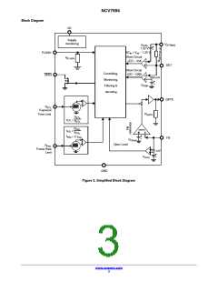
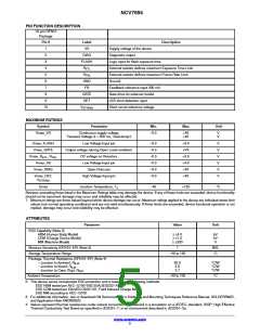
PIN FUNCTION DESCRIPTION
10−pin DFN10
Package
Pin #
Label
VS
Description
1
2
Supply voltage of the device
Diagnostic output
DIAG
FLASH
3
Logic input for flash exposure time
4
R
R
External resistor defines maximum Exposure Time Limit
External resistor defines maximum Frame Rate Limit
Ground
ETL
FRL
5
6
GND
FB
7
Feedback reference input 300 mV.
Gate drive for external mosfet
8
GATE
DET
9
LED short detection input
10
V
Short circuit reference voltage
STRING
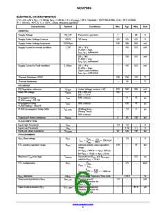
MAXIMUM RATINGS
Symbol
Parameter
Continuous supply voltage
Min.
Max.
Unit
Vmax_VS
−0.3
−
+40
+40
V
V
Transient Voltage (t < 500 ms, “load dump”)
Vmax_FLASH
Vmax_GATE
Low Voltage Input pin
−0.3
−0.3
−0.3
−0.3
−0.3
−0.3
+3.6
+VS
+3.6
+3.6
+40
V
V
V
V
V
V
Output voltage (during Open Load condition)
DC voltage on Resistors
Vmax_R , R
ETL
FRL
Vmax_FB
Low Voltage Input pin
Vmax_DIAG
Open Drain pin
Vmax_DET,
High Voltage Input pin
+40
V
STRING
Tjmax
Junction Temperature, T
−40
+125
°C
J
Stresses exceeding those listed in the Maximum Ratings table may damage the device. If any of these limits are exceeded, device functionality
should not be assumed, damage may occur and reliability may be affected.
1. Maximum ratings are those values beyond which device damage can occur. Maximum ratings applied to the device are individual stress limit
values (not normal operating conditions) and are not valid simultaneously. If these limits are exceeded, device functional operation is not
implied, damage may occur and reliability may be affected.
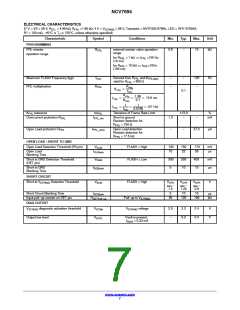
ATTRIBUTES
Parameer
Value
Unit
ESD Capability (Note 2)
HBM (Human Body Model)
≥
≥
≥
4.0
1.0
200
kV
kV
V
CDM (Charge Device Model)
MM (Machine Model)
Moisture Sensitivity (DFN10−EP) (Note 3)
1
MSL
Storage Temperature Range
−40 to 150
°C
Package Thermal Resistance (DFN10−EP) (Note 4)
− Junction to Ambient, R
62.5
5.5
2.7
°C/W
°C/W
°C/W
q
JA
− Junction to Board, R
q
JB
− Junction to Case (Top), R
q
JC
Ambient Temperature
−40 to 105
°C
2. This device series incorporates ESD protection and is tested by the following methods:
ESD HBM tested per AEC−Q100−002 (EIA/JESD22−A114)
ESD CDM tested per EIA/JES D22/C101, Field Induced Charge Model
ESD MM according to AEC−Q100
3. For additional information, see or download ON Semiconductor’s Soldering and Mounting Techniques Reference Manual, SOLDERRM/D,
and Application Note AND8003/D.
4. Values represent thermal resistances under natural convection are obtained in a simulation on a JEDEC−standard, 2S2P; High Effective
Thermal Conductivity Test Board as specified in JESD51−7, in an environment described in JESD51−2a.
www.onsemi.com
5

 ONSEMI [ ONSEMI ]