NCV5171
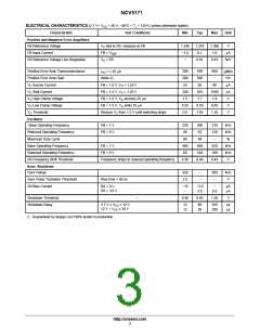
ELECTRICAL CHARACTERISTICS (2.7 V< V < 30 V; −40°C < T < 125°C unless otherwise stated.)
CC
J
Characteristic
Test Conditions
Min
Typ
Max
Unit
Power Switch
Switch Saturation Voltage
Switch Current Limit
I
I
I
I
= 1.5 A, (Note 3)
−
−
−
−
0.8
1.4
−
V
V
V
V
SWITCH
SWITCH
SWITCH
SWITCH
= 1.0 A, 0°C ≤ T ≤ 85°C
0.55
0.75
0.09
J
= 1.0 A, −40°C ≤ T ≤ 0°C
= 10 mA
J
−
0.45
50% duty cycle, (Note 3)
80% duty cycle, (Note 3)
1.6
1.5
1.9
1.7
2.4
2.2
A
A
Minimum Pulse Width
FB = 0 V, I
= 4.0 A, (Note 3)
200
250
300
ns
SW
DI / DIV
CC
2.7 V ≤ V ≤ 12 V, 10 mA ≤ I ≤ 1.0 A
SW
−
−
−
−
10
−
30
100
30
mA/A
mA/A
mA/A
mA/A
SW
CC
12 V < V ≤ 30 V, 10 mA ≤ I
≤ 1.0 A
≤ 1.5 A, (Note 3)
≤ 1.5 A, (Note 3)
SW
CC
SW
2.7 V ≤ V ≤ 12 V, 10 mA ≤ I
CC
SW
17
−
12 V < V ≤ 30 V, 10 mA ≤ I
CC
100
Switch Leakage
General
V
= 40 V, V = 0V
−
2.0
100
8.0
mA
SW
CC
Operating Current
Shutdown Mode Current
I
= 0
−
5.5
mA
SW
V
V
< 0.8 V, SS = 0 V, 2.7 V ≤ V ≤ 12 V
< 0.8 V, SS = 0 V, 12 V ≤ V ≤ 30 V
−
−
12
−
60
mA
C
C
CC
100
CC
Minimum Operation Input Voltage
Thermal Shutdown
V
switching, maximum I
10 mA
SW =
−
150
−
2.45
180
25
2.70
210
−
V
SW
(Note 3)
(Note 3)
°C
°C
Thermal Hysteresis
3. Guaranteed by design, not 100% tested in production.
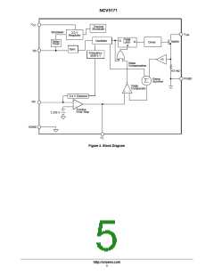
PACKAGE PIN DESCRIPTION
Package
Pin #
Pin
Symbol
Function
1
V
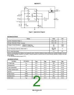
Loop compensation pin. The V pin is the output of the error amplifier and is used for loop compensation,
current limit and soft start. Loop compensation can be implemented by a simple RC network as shown in the
application diagram on page 2 as R1 and C1.
C
C
2
3
4
FB
Test
SS
Positive regulator feedback pin. This pin senses a positive output voltage and is referenced to 1.276 V. When
the voltage at this pin falls below 0.4 V, chip switching frequency reduces to 20% of the nominal frequency.
These pins are connected to internal test logic and should either be left floating or tied to ground. Connection
to a voltage between 2 V and 6 V shuts down the internal oscillator and leaves the power switch running.
Synchronization and shutdown pin. This pin may be used to synchronize the part to nearly twice the base
frequency. A TTL low will shut the part down and put it into low current mode. If synchronization is not used,
this pin should be either tied high or left floating for normal operation.
5
6
V
Input power supply pin. This pin supplies power to the part and should have a bypass capacitor connected to
AGND.
CC
AGND
PGND
Analog ground. This pin provides a clean ground for the controller circuitry and should not be in the path of
large currents. The output voltage sensing resistors should be connected to this ground pin. This pin is
connected to the IC substrate.
7
8
Power ground. This pin is the ground connection for the emitter of the power switching transistor. Connection
to a good ground plane is essential.
V
High current switch pin. This pin connects internally to the collector of the power switch. The open voltage
across the power switch can be as high as 40 V. To minimize radiation, use a trace as short as practical.
SW
http://onsemi.com
4

 ONSEMI [ ONSEMI ]