NCV5171
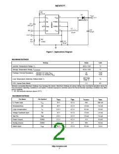
R2
3.72 k
D1
V
OUT
8
1
2
3
4
V
5 V
V
SW
C
MBRS120T3
7
6
5
PGND
FB
C1
0.01 mF
AGND
Test
SS
L1
+
C3
22 mF
SS
V
CC
22 mH
3.3 V
R3
R1
5 k
+
C2
22 mF
1.28 k
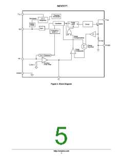
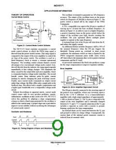
Figure 1. Applications Diagram
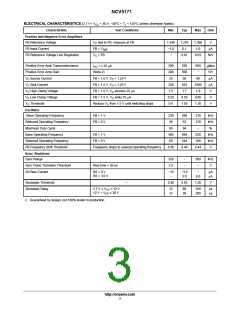
MAXIMUM RATINGS
Rating
Value
Unit
°C
Junction Temperature Range, T
Storage Temperature Range, T
−40 to +150
−65 to +150
J
°C
STORAGE
Package Thermal Resistance,
Junction−to−Case, R
Junction−to−Ambient, R
45
165
°C/W
°C/W
q
JC
q
JA
260 Peak
(Note 1)
Lead Temperature Soldering: Reflow (Note 1)
ESD, Human Body Model
°C
1.2
kV
Stresses exceeding Maximum Ratings may damage the device. Maximum Ratings are stress ratings only. Functional operation above the
Recommended Operating Conditions is not implied. Extended exposure to stresses above the Recommended Operating Conditions may affect
device reliability.
1. 60−180 seconds minimum above 237°C.
MAXIMUM RATINGS
Pin Name
IC Power Input
Pin Symbol
V
V
I
I
SINK
MAX
MIN
SOURCE
V
35 V
30 V
6.0 V
10 V
6.0 V
0.3 V
0 V
−0.3 V
−0.3 V
−0.3 V
−0.3 V
−0.3 V
−0.3 V
0 V
N/A
200 mA
1.0 mA
10 mA
1.0 mA
1.0 mA
10 mA
10 mA
3.0 A
CC
Shutdown/Sync
Loop Compensation
Voltage Feedback Input
Test Pin
SS
1.0 mA
10 mA
1.0 mA
1.0 mA
4 A
V
C
FB
Test
Power Ground
Analog Ground
Switch Input
PGND
AGND
N/A
V
40 V
−0.3 V
10 mA
SW
http://onsemi.com
2

 ONSEMI [ ONSEMI ]