NCP698
APPLICATIONS INFORMATION
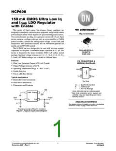
A typical application circuit for the NCP698 is shown in
Figure 1.
on the PCB, the board material and also the ambient
temperature effect the rate of temperature rise for the part.
This is stating that when the devices have good thermal
conductivity through the PCB, the junction temperature will
be relatively low with high power dissipation applications.
The maximum dissipation the package can handle is
given by:
Input Decoupling (C1)
A 1.0 ꢀ F capacitor either ceramic or tantalum is
recommended and should be connected close to the NCP698
package. Higher values and lower ESR will improve the
overall line transient response.
T
*T
A
J(max)
R
TDK capacitor: C2012X5R1C105K, or C1608X5R1A105K
PD +
ꢁJA
Output Decoupling (C2)
If junction temperature is not allowed above the
maximum 125°C, then the NCP698 can dissipate up to
250 mW @ 25°C.
The NCP698 is a very stable regulator and does not
require any specific Equivalent Series Resistance (ESR) or
a minimum output current. Capacitors exhibiting ESRs
ranging from a few mꢂ up to 10 ꢂ can thus safely be used.
The minimum decoupling value is 0.1 ꢀ F and can be
augmented to fulfill stringent load transient requirements.
The regulator accepts ceramic chip capacitors as well as
tantalum devices. Larger values improve noise rejection and
load regulation transient response.
The power dissipated by the NCP698 can be calculated
from the following equation:
[
]
[
]
* I
in out out
P
tot
+ V * I
ꢀ(I ) ) V * V
in gnd out
or
)
*
I
P
V
tot
I
out out
) I
V
+
inMAX
gnd
out
TDK capacitor: C2012X5R1C105K, C1608X5R1A105K,
or C3216X7R1C105K
If an 80 mA output current is needed then the ground
current from the data sheet is 2.5 ꢀ A. For an NCP698
(3.0 V), the maximum input voltage will then be 6.0 V.
Enable Operation
The enable pin will turn on the regulator when pulled high
and turn off the regulator when pulled low. These limits of
threshold are covered in the electrical specification section
of this data sheet. If the enable is not used, then the pin
350
330
310
290
should be connected to V .
in
Hints
270
No pin connected to Cu Plane
Please be sure the Vin and GND lines are sufficiently
wide. When the impedance of these lines is high, there is a
chance to pick up noise or cause the regulator to
malfunction.
Place external components, especially the output
capacitor, as close as possible to the circuit, and make leads
as short as possible.
250
230
210
190
Pin 2 connected to Cu Plane
170
150
0
100
200
300
400
500
600 700
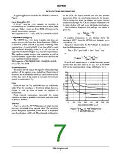
Thermal
2
PCB COPPER AREA (mm )
As power across the NCP698 increases, it might become
necessary to provide some thermal relief. The maximum
power dissipation supported by the device is dependent
upon board design and layout. Mounting pad configuration
Figure 12. RqJA vs. Pad Copper Area
(1 oz Cu thickness)
http://onsemi.com
7

 ONSEMI [ ONSEMI ]