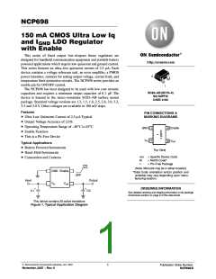
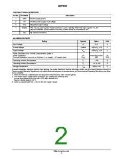
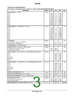
NCP698
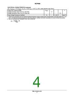
6
5
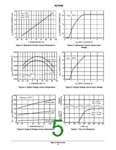
60
I
= 1 mA to 30 mA
= 4.0 V
OUT
30
0
V
IN
4
3
1
-30
1
V
= 3.0 V
OUT
0.5
0
0.5
0
C
= 0.1 ꢀ F
OUT
V
OUT
= 3.0 V
C
= 0.1 ꢀ F
= 10 mA
-0.5
-1
-0.5
-1
OUT
I
OUT
0
50 100 150 200 250 300 350 400 450 500
t, TIME (ꢀ s)
0
50 100 150 200 250 300 350 400 450 500
t, TIME (ꢀ s)
Figure 8. Line Transient Response
Figure 9. Load Transient Response
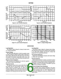
60
3.5
3
I
= 1 mA to 30 mA
= 4.0 V
OUT
V
V
= 5.0 V
= 3.0 V
= 50 mA
30
0
IN
V
IN
OUT
I
OUT
2.5
2
C
OUT
= 0.1 ꢀ F
-30
400
1.5
1
200
0
C
= 1.0 ꢀ F
= 3.0 V
OUT
0.5
0
-200
V
OUT
-400
0
100 200 300 400 500 600 700 800 900 1000
0.01
0.1
1
10
100
1000
t, TIME (ꢀ s)
f, FREQUENCY (kHz)
Figure 10. Load Transient Response
Figure 11. Output Voltage Noise
DEFINITIONS
Load Regulation
Line Regulation
The change in output voltage for a change in output current
at a constant temperature.
The change in output voltage for a change in input voltage.
The measurement is made under conditions of low dissipation
or by using pulse technique such that the average chip
temperature is not significantly affected.
Dropout Voltage
The input/output differential at which the regulator output
no longer maintains regulation against further reductions in
input voltage. Measured when the output drops 3.0% below
its nominal. The junction temperature, load current, and
minimum input supply requirements affect the dropout level.
Line Transient Response
Typical over and undershoot response when input voltage
is excited with a given slope.
Thermal Protection
Internal thermal shutdown circuitry is provided to protect
the integrated circuit in the event that the maximum junction
temperature is exceeded. When activated at typically 160°C,
the regulator turns off. This feature is provided to prevent
failures from accidental overheating.
Maximum Power Dissipation
The maximum total dissipation for which the regulator
will operate within its specifications.
Quiescent Current
The quiescent current is the current which flows through
the ground when the LDO operates without a load on its
output: internal IC operation, bias, etc. When the LDO
becomes loaded, this term is called the Ground current. It is
actually the difference between the input current (measured
through the LDO input pin) and the output current.
Maximum Package Power Dissipation
The maximum power package dissipation is the power
dissipation level at which the junction temperature reaches its
maximum operating value, i.e. 125°C. Depending on the
ambient power dissipation and thus the maximum available
output current.
http://onsemi.com
6

 ONSEMI [ ONSEMI ]