NCP1236
ELECTRICAL CHARACTERISTICS
(For typical values T = 25C, for min/max values T = −40C to +125C, V = 125 V, V = 11 V unless otherwise noted)
J
J
HV
CC
Characteristics
Test Condition
Symbol
Min
Typ
Max
Unit
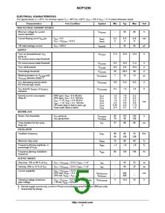
HIGH VOLTAGE CURRENT SOURCE
Minimum voltage for current
source operation
V
−
30
60
V
HV(min)
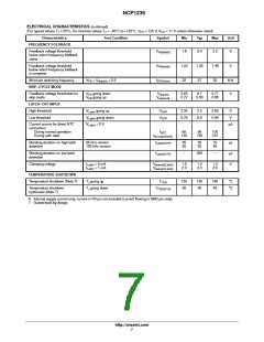
Current flowing out of V pin
V
CC
V
CC
= 0 V
I
I
0.2
3
0.5
6
0.8
9
mA
CC
start1
start2
= V
− 0.5 V
CC(on)
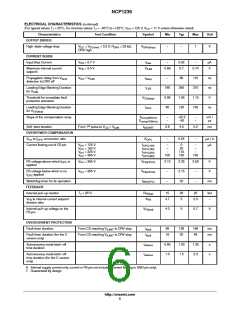
Off−state leakage current
V
HV
= 500 V
I
−
25
50
mA
start(off)
SUPPLY
Turn−on threshold level, V
V
CC(on)
11.0
12.0
13.0
V
CC
going up
HV current source stop threshold
HV current source restart threshold
Turn−off threshold
V
V
9.5
8.5
25
7
10.5
9.5
11.5
10.5
28
V
V
CC(min)
V
CC(off)
Overvoltage threshold
26.5
10
V
CC(ovp)
Blanking duration on V
CC(ovp)
and
t
13
ms
CC(off)
VCC(blank)
V
detection (Note 7)
V
decreasing level at which
V
3.6
0.4
5.0
1.0
6.0
1.6
V
V
CC
CC(reset)
the internal logic resets
level for I to I
START2
V
CC
V
START1
CC(inhibit)
transition
Internal current consumption
(Note 6)
DRV open, V = 3 V, 65 kHz
I
I
I
I
I
I
1.2
1.2
1.9
2.2
0.67
0.4
1.8
1.9
2.5
2.9
0.9
0.7
2.2
2.3
3.2
3.6
1.13
1.0
FB
CC1
CC1
CC2
CC2
CC3
CC4
DRV open, V = 3 V, 100 kHz
FB
FB
C
C
= 1 nF, V = 3 V, 65 kHz
drv
drv
mA
= 1 nF, V = 3 V, 100 kHz
FB
Off mode (skip or before start−up)
Fault mode (fault or latch)
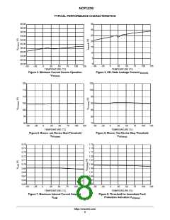
BROWN−OUT
Brown−Out thresholds
V
HV
V
HV
going up
going down
V
92
79
107
92
122
105
V
HV(start)
V
HV(stop)
Timer duration for line cycle
drop−out
t
47
68
90
ms
HV
OSCILLATOR
Oscillator frequency
f
60
92
65
100
70
108
kHz
OSC
Maximum duty cycle
D
75
80
85
%
%
MAX
Frequency jittering amplitude, in
A
$4
$6
$8
jitter
percentage of F
OSC
Frequency jittering modulation
frequency
F
jitter
85
125
165
Hz
OUTPUT DRIVER
Rise time, 10% to 90 % of V
V
V
V
= V
= V
= V
+ 0.2 V, C
+ 0.2 V, C
= 1 nF
t
−
−
40
40
70
70
ns
ns
CC
CC
CC
CC
CC(min)
CC(min)
CC(min)
DRV
DRV
DRV
rise
Fall time, 90% to 10 % of V
Current capability
= 1 nF
= 1 nF
t
fall
CC
+ 0.2 V, C
= 0 V
DRV high, V
I
−
−
500
500
−
−
mA
V
DRV
DRV(source)
DRV(sink)
DRV low, V
= V
I
DRV
CC
Clamping voltage (maximum
gate voltage)
V
CC
= V
– 0.2 V, DRV high, R
= 220 pF
V
11
13.5
16
CCmax
DRV
DRV(clamp)
= 33 kW, C
load
6. Internal supply current only, current in FB pin not included (current flowing in GND pin only).
7. Guaranteed by design.
http://onsemi.com
5

 ONSEMI [ ONSEMI ]