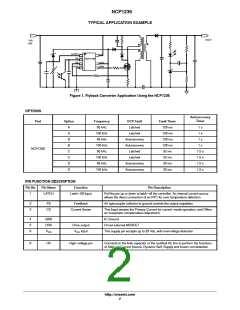
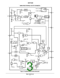
NCP1236
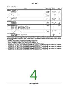
MAXIMUM RATINGS
Rating
Symbol
Value
Unit
Supply Pin (pin 6) (Note 2)
Voltage range
V
–0.3 to 28
$30
V
mA
CCMAX
CCMAX
Current range
I
High Voltage Pin (pin 8) (Note 2)
Voltage range
V
–0.3 to 500
V
mA
HVMAX
HVMAX
Current range
I
$20
Driver Pin (pin 5) (Note 2)
Voltage range
V
–0.3 to 20
$1000
V
mA
DRVMAX
DRVMAX
Current range
I
All other pins (Note 2)
Voltage range
V
–0.3 to 10
$10
V
mA
MAX
MAX
Current range
I
Thermal Resistance SOIC−7
R
C/W
J−A
Junction−to−Air, low conductivity PCB (Note 3)
Junction−to−Air, medium conductivity PCB (Note 4)
Junction−to−Air, high conductivity PCB (Note 5)
162
147
115
Temperature Range
C
Operating Junction Temperature
Storage Temperature Range
T
−40 to +150
−60 to +150
JMAX
STRGMAX
T
ESD Capability (Note 1)
V
Human Body Model (All pins except HV)
Machine Model
2000
200
Stresses exceeding Maximum Ratings may damage the device. Maximum Ratings are stress ratings only. Functional operation above the
Recommended Operating Conditions is not implied. Extended exposure to stresses above the Recommended Operating Conditions may affect
device reliability.
1. This device series contains ESD protection and exceeds the following tests:
Human Body Model 2000 V per JEDEC standard JESD22, Method A114E
Machine Model Method 200 V per JEDEC standard JESD22, Method A115A
2. This device contains latch−up protection and exceeds 100 mA per JEDEC Standard JESD78
2
3. As mounted on a 80 x 100 x 1.5 mm FR4 substrate with a single layer of 50 mm of 2 oz copper traces and heat spreading area. As specified
for a JEDEC 51−1 conductivity test PCB. Test conditions were under natural convection or zero air flow.
2
4. As mounted on a 80 x 100 x 1.5 mm FR4 substrate with a single layer of 100 mm of 2 oz copper traces and heat spreading area. As specified
for a JEDEC 51−2 conductivity test PCB. Test conditions were under natural convection or zero air flow.
2
5. As mounted on a 80 x 100 x 1.5 mm FR4 substrate with a single layer of 650 mm of 2 oz copper traces and heat spreading area. As specified
for a JEDEC 51−3 conductivity test PCB. Test conditions were under natural convection or zero air flow.
http://onsemi.com
4

 ONSEMI [ ONSEMI ]