NCP1200
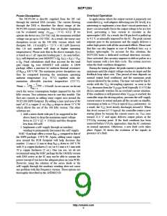
8
7
6
5
1
2
3
4
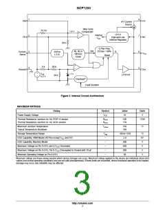
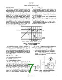
Adj
FB
HV
NC
HV Current
Source
Skip Cycle
Comparator
75.5 k
1.4 V
+
UVLO
Internal
−
High and Low
Internal Regulator
V
CC
29 k
Q Flip−Flop
DCmax = 80%
Set
40, 60 or
100 kHz
Clock
Q
Current
Sense
250 ns
L.E.B.
V
CC
Reset
+
−
8 k
60 k
Ground
Drv
+
−
V
5.2 V
1 V
ref
±110 mA
20 k
Overload?
Fault Duration
Figure 2. Internal Circuit Architecture
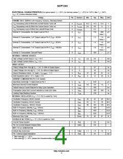
MAXIMUM RATINGS
Rating
Symbol
Value
Units
V
Power Supply Voltage
V
R
16
CC
Thermal Resistance Junction−to−Air, PDIP−8 version
Thermal Resistance Junction−to−Air, SOIC version
100
178
°C/W
q
q
JA
JA
R
Maximum Junction Temperature
Typical Temperature Shutdown
T
150
140
°C
Jmax
−
Storage Temperature Range
T
−60 to +150
°C
kV
V
stg
ESD Capability, HBM Model (All Pins except V and HV)
−
−
−
−
−
2.0
200
450
500
30
CC
ESD Capability, Machine Model
Maximum Voltage on Pin 8 (HV), pin 6 (V ) Grounded
V
CC
Maximum Voltage on Pin 8 (HV), Pin 6 (V ) Decoupled to Ground with 10 mF
V
CC
Minimum Operating Voltage on Pin 8 (HV)
V
Maximum ratings are those values beyond which device damage can occur. Maximum ratings applied to the device are individual stress limit
values (not normal operating conditions) and are not valid simultaneously. If these limits are exceeded, device functional operation is not implied,
damage may occur and reliability may be affected.
http://onsemi.com
3

 ONSEMI [ ONSEMI ]