NCP1200
Power Dissipation
Overload Operation
The NCP1200 is directly supplied from the DC rail
through the internal DSS circuitry. The current flowing
through the DSS is therefore the direct image of the
NCP1200 current consumption. The total power dissipation
can be evaluated using: (VHVDC * 11 V) @ ICC2. If we
operate the device on a 250 VAC rail, the maximum rectified
voltage can go up to 350 VDC. As a result, the worse case
dissipation occurs on the 100 kHz version which will
dissipate 340 . 1.8 mA@Tj = −25°C = 612 mW (however
this 1.8 mA number will drop at higher operating
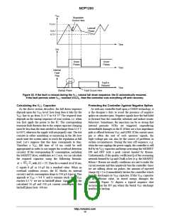
In applications where the output current is purposely not
controlled (e.g. wall adapters delivering raw DC level), it is
interesting to implement a true short−circuit protection. A
short−circuit actually forces the output voltage to be at a low
level, preventing a bias current to circulate in the
optocoupler LED. As a result, the FB pin level is pulled up
to 4.1 V, as internally imposed by the IC. The peak current
setpoint goes to the maximum and the supply delivers a
rather high power with all the associated effects. Please note
that this can also happen in case of feedback loss, e.g. a
broken optocoupler. To account for this situation, the
NCP1200 hosts a dedicated overload detection circuitry.
Once activated, this circuitry imposes to deliver pulses in a
burst manner with a low duty cycle. The system recovers
when the fault condition disappears.
temperatures). Please note that in the above example, I
CC2
is based on a 1 nF capacitor loading pin 5. As seen before,
will depend on your MOSFET’s Q : I = I + F
I
CC2
g
CC2
CC1
sw
x Q . Final calculations shall thus account for the total
g
gate−charge Q your MOSFET will exhibit. A DIP8
g
During the startup phase, the peak current is pushed to the
maximum until the output voltage reaches its target and the
feedback loop takes over. This period of time depends on
normal output load conditions and the maximum peak
current allowed by the system. The time−out used by this IC
package offers a junction−to−ambient thermal resistance
of R
100°C/W. The maximum power dissipation can
qJ−A
thus be computed knowing the maximum operating
ambient temperature (e.g. 70°C) together with the
maximum allowable junction temperature (125°C):
TJmax * TAmax
works with the V decoupling capacitor: as soon as the
CC
Pmax +
= 550 mW. As we can see, we do not
V
CC
decreases from the V
level (typically 11.4 V) the
RRqJ*A
CCOFF
device internally watches for an overload current situation.
If this condition is still present when V is reached, the
controller stops the driving pulses, prevents the self−supply
current source to restart and puts all the circuitry in standby,
reach the worse consumption budget imposed by the 100
kHz version. Two solutions exist to cure this trouble. The
first one consists in adding some copper area around the
CCON
NCP1200 DIP8 footprint. By adding a min−pad area of 80
2
consuming as little as 350 mA typical (I parameter). As
mm of 35 m copper (1 oz.) R
drops to about 75°C/W
CC3
qJ−A
a result, the V level slowly discharges toward 0. When
which allows the use of the 100 kHz version. The other
solutions are:
CC
this level crosses 6.3 V typical, the controller enters a new
startup phase by turning the current source on: V rises
1. Add a series diode with pin 8 (as suggested in the
above lines) to drop the maximum input voltage
down to 222 V ((2 350)/pi) and thus dissipate
less than 400 mW
CC
toward 11.4 V and again delivers output pulses at the
UVLO crossing point. If the fault condition has been
H
removed before UVLO approaches, then the IC continues
L
its normal operation. Otherwise, a new fault cycle takes
place. Figure 20 shows the evolution of the signals in
presence of a fault.
2. Implement a self−supply through an auxiliary
winding to permanently disconnect the self−supply.
SOIC−8 package offers a worse R
compared to that of
qJ−A
the DIP8 package: 178°C/W. Again, adding some copper
area around the PCB footprint will help decrease this
number: 12 mm x 12 mm to drop R
down to 100°C/W
qJ−A
with 35 m copper thickness (1 oz.) or 6.5 mm x 6.5 mm with
70 m copper thickness (2 oz.). One can see, we do not
recommend using the SOIC package for the 100 kHz version
with DSS active as the IC may not be able to sustain the
power (except if you have the adequate place on your PCB).
However, using the solution of the series diode or the
self−supply through the auxiliary winding does not cause
any problem with this frequency version. These options are
thoroughly described in the AND8023/D.
http://onsemi.com
9

 ONSEMI [ ONSEMI ]