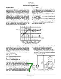
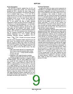
NCP1200
*
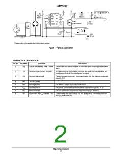
6.5 V @ 600 mA
C2
470 mF/10 V
C3
10 mF
400 V
+
+
D2
1N5819
HV
NC
1
2
3
4
8
7
6
5
Adj
FB
CS
V
CC
M1
MTD1N60E
Rf
GND Drv
470
EMI
Filter
+
C5
R
sense
10 mF
D8
5 V1
Universal Input
*Please refer to the application information section
Figure 1. Typical Application
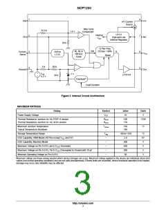
PIN FUNCTION DESCRIPTION
Pin No. Pin Name
Function
Description
1
2
3
Adj
FB
CS
Adjust the Skipping Peak Current
This pin lets you adjust the level at which the cycle skipping process takes
place.
Sets the Peak Current Setpoint
Current Sense Input
By connecting an Optocoupler to this pin, the peak current setpoint is ad-
justed accordingly to the output power demand.
This pin senses the primary current and routes it to the internal comparator
via an L.E.B.
4
5
6
7
8
GND
Drv
The IC Ground
Driving Pulses
Supplies the IC
No Connection
The driver’s output to an external MOSFET.
V
CC
This pin is connected to an external bulk capacitor of typically 10 mF.
This un−connected pin ensures adequate creepage distance.
Connected to the high−voltage rail, this pin injects a constant current into
NC
HV
Generates the V from the Line
CC
the V bulk capacitor.
CC
http://onsemi.com
2

 ONSEMI [ ONSEMI ]