NCP1050, NCP1051, NCP1052, NCP1053, NCP1054, NCP1055
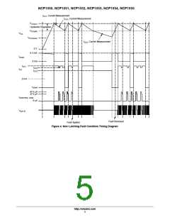
+
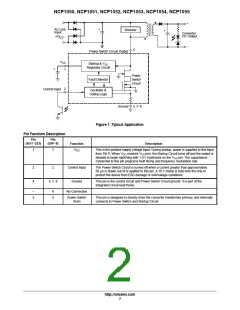
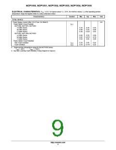
AC Line
Input
+
Snubber
+
Converter
DC Output
−
5
Power Switch Circuit Output
V
CC
Startup & V
CC
Regulator Circuit
+
1
Power
Switch
Circuit
Fault Detector
2
Control Input
Oscillator &
Gating Logic
Ground 3, 7−8
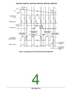
Figure 1. Typical Application
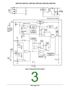
Pin Function Description
Pin
Pin
(SOT−223)
(DIP−8)
Function
Description
This is the positive supply voltage input. During startup, power is supplied to this input
1
1
V
CC
from Pin 5. When V reaches V (on), the Startup Circuit turns off and the output is
CC
CC
allowed to begin switching with 1.0 V hysteresis on the V pin. The capacitance
CC
connected to this pin programs fault timing and frequency modulation rate.
2
4
2
Control Input
The Power Switch Circuit is turned off when a current greater than approximately
50 m A is drawn out of or applied to this pin. A 10 V clamp is built onto the chip to
protect the device from ESD damage or overvoltage conditions.
3, 7, 8
Ground
This pin is the control circuit and Power Switch Circuit ground. It is part of the
integrated circuit lead frame.
−
3
4
5
No Connection
Power Switch
Drain
This pin is designed to directly drive the converter transformer primary, and internally
connects to Power Switch and Startup Circuit.
http://onsemi.com
2

 ONSEMI [ ONSEMI ]