NCP1050, NCP1051, NCP1052, NCP1053, NCP1054, NCP1055
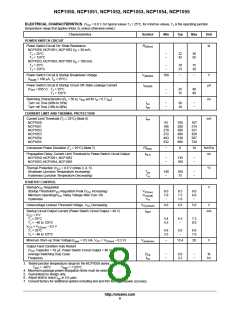
ELECTRICAL CHARACTERISTICS (V = 8.0 V, for typical values T = 25°C, for min/max values, T is the operating junction
CC
J
J
temperature range that applies (Note 8), unless otherwise noted.)
Characteristics
TOTAL DEVICE
Symbol
Min
Typ
Max
Unit
Power Supply Current After UVLO Turn−On (Note 9)
Power Switch Circuit Enabled
NCP1050, NCP1051, NCP1052
A Suffix Device
mA
I
CC1
0.35
0.40
0.40
0.45
0.50
0.525
0.55
0.60
0.65
B Suffix Device
C Suffix Device
NCP1053, NCP1054, NCP1055
A Suffix Device
0.40
0.45
0.50
0.50
0.575
0.65
0.60
0.70
0.80
B Suffix Device
C Suffix Device
Power Switch Circuit Disabled
Non−Fault Condition
Fault Condition
I
I
0.35
0.10
0.45
0.175
0.55
0.25
CC2
CC3
8. Tested junction temperature range for the NCP105X series:
T
low
= −40°C
T
high
= +125°C
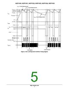
9. See Non−Latching Fault Condition Timing Diagram in Figure 4.
http://onsemi.com
9

 ONSEMI [ ONSEMI ]