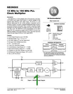
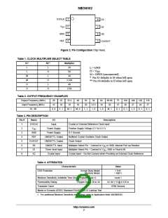
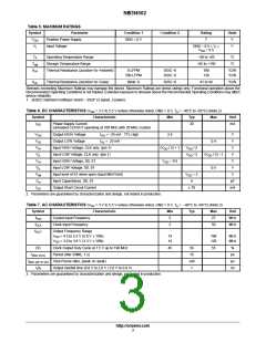
NB3N502
APPLICATIONS INFORMATION
High Frequency CMOS/TTL Oscillators
Series Termination Resistor Recommendation
A 33 W series terminating resistor can be used on the
CLKOUT pin.
The NB3N502, along with a low frequency fundamental
mode crystal, can build a high frequency CMOS/TTL output
oscillator. For example, a 20 MHz crystal connected to the
NB3N502 with the 5X output selected (S1 = L, S0 = H)
produces a 100 MHz CMOS/TTL output clock.
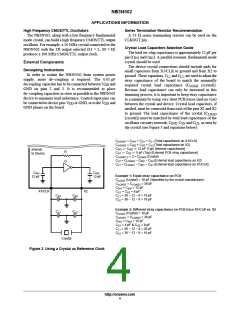
Crystal Load Capacitors Selection Guide
The total on−chip capacitance is approximately 12 pF per
pin (C and C ). A parallel resonant, fundamental mode
IN1
IN2
crystal should be used.
External Components
The device crystal connections should include pads for
small capacitors from X1/CLK to ground and from X2 to
Decoupling Instructions
In order to isolate the NB3N502 from system power
supply, noise de−coupling is required. The 0.01 mF
ground. These capacitors, C and C , are used to adjust the
L1
L2
stray capacitance of the board to match the nominally
required crystal load capacitance (C (crystal)).
decoupling capacitor has to be connected between V and
DD
LOAD
GND on pins 2 and 3. It is recommended to place
de−coupling capacitors as close as possible to the NB3N502
device to minimize lead inductance. Control input pins can
be connected to device pins V or GND, or to the V and
GND planes on the board.
Because load capacitance can only be increased in this
trimming process, it is important to keep stray capacitance
to a minimum by using very short PCB traces (and no vias)
between the crystal and device. Crystal load capacitors, if
needed, must be connected from each of the pins X1 and X2
DD
DD
to ground. The load capacitance of the crystal (C
LOAD
(crystal)) must be matched by total load capacitance of the
oscillator circuitry network, C , C and C , as seen by
INX SX
LX
the crystal (see Figure 3 and equations below).
C
C
C
C
C
C
C
= C
= C
+ C + C [Total capacitance on X1/CLK]
S1 L1
LOAD1
LOAD2
IN1
IN1
+ C + C [Total capacitance on X2]
IN2
S2
L2
[ C
[ 12 pF (Typ) [Internal capacitance]
IN2
Internal
to Device
R
[ C [ 5 pF (Typ) [External PCB stray capacitance]
S1
S2
= 2 S C
(Crystal)
LOAD1,2
LOAD
= C
= C
− C
− C
− C [External load capacitance on X2]
S2
− C [External load capacitance on X1/CLK]
S1
G
L2
L1
LOAD2
LOAD1
IN2
IN1
C
12 pF
C
IN2
12 pF
IN1
Example 1: Equal stray capacitance on PCB
C
C
C
C
C
C
(Crystal) = 18 pF (Specified by the crystal manufacturer)
LOAD
= C
= 36 pF
LOAD1
LOAD2
= C
= 12 pF
IN1
S1
IN2
X2
X1/CLK
= C = 6 pF
S2
C
S1
C
S2
= 36 − 12 − 6 = 18 pF
= 36 − 12 − 6 = 18 pF
L1
L2
Example 2: Different stray capacitance on PCB trace X1/CLK vs. X2
C
L1
C
L2
C
C
C
C
C
C
(Crystal) = 18 pF
LOAD
= C
= 36 pF
LOAD1
LOAD2
= C
= 12 pF
IN1
S1
IN2
= 4 pF & C = 8 pF
S2
= 36 − 12 − 4 = 20 pF
= 36 − 12 − 8 = 16 pF
L1
L2
Crystal
Figure 3. Using a Crystal as Reference Clock
http://onsemi.com
4

 ONSEMI [ ONSEMI ]