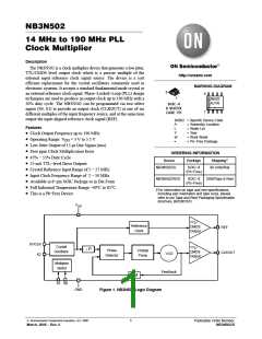
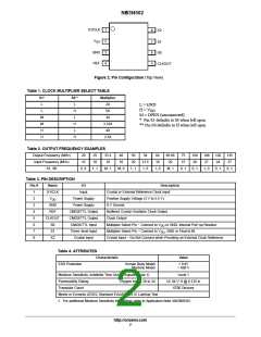
NB3N502
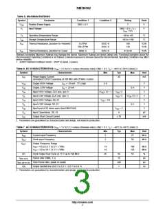
Table 5. MAXIMUM RATINGS
Symbol
Parameter
Condition 1
Condition 2
Rating
Units
V
Positive Power Supply
Input Voltage
GND = 0 V
7
V
V
DD
V
GND – 0.5 = V =
I
I
V
+ 0.5
DD
T
Operating Temperature Range
−40 to +85
°C
°C
A
T
stg
Storage Temperature Range
−65 to +150
q
Thermal Resistance (Junction−to−Ambient)
0 LFPM
SOIC−8
SOIC−8
190
130
°C/W
°C/W
JA
500 LFPM
q
Thermal Resistance (Junction−to−Case)
(Note 1)
SOIC−8
41 to 44
°C/W
JC
Stresses exceeding Maximum Ratings may damage the device. Maximum Ratings are stress ratings only. Functional operation above the
Recommended Operating Conditions is not implied. Extended exposure to stresses above the Recommended Operating Conditions may affect
device reliability.
1. JEDEC standard multilayer board − 2S2P (2 signal, 2 power).
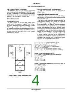
Table 6. DC CHARACTERISTICS (V = 3 V to 5.5 V unless otherwise noted, GND = 0 V, T = −40°C to +85°C) (Note 2)
DD
A
Symbol
Characteristic
Min
Typ
Max
Unit
I
Power Supply Current
(unloaded CLKOUT operating at 100 MHz with 20 MHz crystal)
20
mA
DD
V
Output HIGH Voltage
Output LOW Voltage
I
I
= −25 mA TTL High
= 25 mA
2.4
V
V
OH
OH
OL
V
0.4
OL
V
Input HIGH Voltage, CLK only (pin 1)
Input LOW Voltage, CLK only (pin 1)
Input HIGH Voltage, S0, S1
(V / 2) + 1
V
V
/ 2
V
IH
DD
DD
DD
V
/ 2
(V / 2) −1
DD
V
IL
V
V
– 0.5
DD
V
IH
V
V
Input LOW Voltage, S0, S1
0.5
V
IL
Input level of S1 when open (Input Mid Point)
Input Capacitance, S0, S1
V
÷ 2
DD
V
IM
C
4
pF
mA
in
I
Output Short Circuit Current
± 70
SC
2. Parameters are guaranteed by characterization and design, not tested in production.
Table 7. AC CHARACTERISTICS (V = 3 V to 5.5 V unless otherwise noted, GND = 0 V, T = −40°C to +85°C) (Note 3)
DD
A
Symbol
Characteristic
Min
5
Typ
Max
27
Unit
MHz
MHz
f
Crystal Input Frequency
Clock Input Frequency
Xtal
f
2
50
CLK
f
Output Frequency Range
OUT
V
V
= 4.5 to 5.5 V (5.0 V ± ±10%)
= 3.0 to 3.6 V (3.3 V ± ±10%)
14
14
190
120
MHz
MHz
DD
DD
DC
Clock Output Duty Cycle at 1.5 V up to 190 MHz
Period Jitter (RMS, 1 σ)
45
50
15
± 40
1
55
%
ps
ps
ns
t
jitter (rms)
jitter (pk−to−pk)
t
Total Period Jitter, (peak−to−peak)
t /t
r
Output rise/fall time (0.8 V to 2.0 V / 2.0 V to 0.8 V)
f
3. Parameters are guaranteed by characterization and design, not tested in production.
http://onsemi.com
3

 ONSEMI [ ONSEMI ]