NB3N502
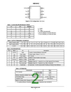
X1/CLK
1
X2
8
V
2
3
4
DD
7
6
5
S1
GND
REF
S0
CLKOUT
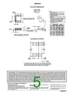
Figure 2. Pin Configuration (Top View)
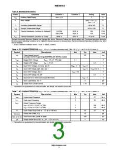
Table 1. CLOCK MULTIPLIER SELECT TABLE
S1*
L
S0**
L
Multiplier
2X
L = GND
H = V
L
H
5X
DD
M = OPEN (unconnected)
* Pin S1 defaults to M when left open
** Pin S0 defaults to H when left open
M
M
H
L
3X
H
3.33X
4X
L
H
H
2.5X
Table 2. OUTPUT FREQUENCY EXAMPLES
Output Frequency (MHz)
Input Frequency (MHz)
S1, S0
20
10
25
10
33.3
10
48
16
50
20
54
64
16
66.66
20
75
15
100
20
108
27
120
24
135
27
13.5
1, 0
0 ,0
1, 1
M, 1
M, 0
1, 1
1, 0
M, 1
0, 1
0, 1
1, 0
0, 1
0, 1
Table 3. PIN DESCRIPTION
Pin #
Name
I/O
Description
1
2
3
4
5
6
7
8
X1/CLK
Input
Crystal or External Reference Clock Input
Positive Supply Voltage (3 V to 5.5 V)
0 V Ground.
V
Power Supply
Power Supply
DD
GND
REF
CLKOUT
S0
CMOS/TTL Output
CMOS/TTL Output
CMOS/TTL Input
Three−level Input
Crystal Input
Buffered Crystal Oscillator Clock Output
Clock Output
Multiplier Select Pin − Connect to V or GND. Internal Pull−up Resistor.
DD
S1
Multiplier Select Pin − Connect to V , GND or Float to M.
DD
X2
Crystal Input − Do Not Connect when Providing an External Clock Reference
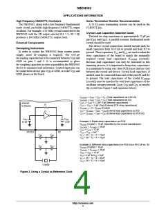
Table 4. ATTRIBUTES
Characteristic
Value
ESD Protection
Human Body Model
Machine Model
> 8 kV
> 600 V
Moisture Sensitivity, Indefinite Time Out of Drypack (Note 1)
Level 1
Flammability Rating
Transistor Count
Oxygen Index: 28 to 34
UL 94 V−0 @ 0.125 in
6700 Devices
Meets or Exceeds JEDEC Standard EIA/JESD78 IC Latchup Test
1. For additional Moisture Sensitivity information, refer to Application Note AND8003/D.
http://onsemi.com
2

 ONSEMI [ ONSEMI ]