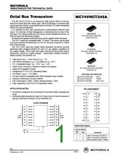
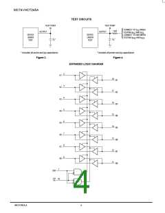
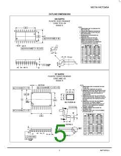
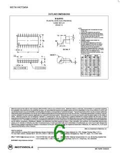
MC74VHCT245A
MAXIMUM RATINGS*
V
DC Supply Voltage
DC Input Voltage
DC Output Voltage
– 0.5 to + 7.0
– 0.5 to + 7.0
– 0.5 to + 7.0
V
V
V
This device contains protection
circuitry to guard against damage
due to high static voltages or electric
fields. However, precautions must
be taken to avoid applications of any
voltage higher than maximum rated
voltages to this high–impedance cir-
CC
V
in
V
Outputs in 3–State
I/O
High or Low State – 0.5 to V
CC
+ 0.5
I
I
Input Diode Current
– 20
mA
mA
mA
mA
mW
IK
cuit. For proper operation, V and
in
Output Diode Current (V
< GND; V
OUT
> V )
CC
± 20
± 25
± 75
OK
OUT
V
should be constrained to the
out
I
DC Output Current, per Pin
DC Supply Current, V and GND Pins
out
range GND (V or V
)
V
.
in out
CC
Unused inputs must always be
tied to an appropriate logic voltage
I
CC
CC
P
Power Dissipation in Still Air,
SOIC Packages†
TSSOP Package†
500
450
D
level (e.g., either GND or V
).
CC
Unused outputs must be left open.
T
stg
Storage Temperature
– 65 to + 150
C
* Absolute maximum continuous ratings are those values beyond which damage to the device
may occur. Exposure to these conditions or conditions beyond those indicated may adversely
affect device reliability. Functional operation under absolute–maximum–rated conditions is not
implied.
†Derating — SOIC Packages: – 7 mW/ C from 65 to 125 C
TSSOP Package: – 6.1 mW/ C from 65 to 125 C
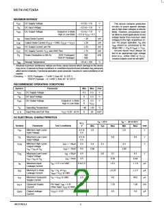
RECOMMENDED OPERATING CONDITIONS
Symbol
Parameter
Min
4.5
0
Max
5.5
5.5
5.5
Unit
V
V
CC
DC Supply Voltage
DC Input Voltage
DC Output Voltage
V
in
V
V
I/O
Outputs in 3–State
High or Low State
0
0
V
V
CC
T
Operating Temperature
Input Rise and Fall Time
– 40
0
+ 85
20
C
A
t , t
r f
V
CC
=5.0V ±0.5V
ns/V
DC ELECTRICAL CHARACTERISTICS
T
A
= 25°C
T = – 40 to 85°C
A
V
CC
V
Symbol
Parameter
Test Conditions
Unit
Min
Typ
Max
Min
Max
V
IH
Minimum High–Level
Input Voltage
4.5 to
5.5
2.0
2.0
V
V
Maximum Low–Level
Input Voltage
4.5 to
5.5
0.8
0.8
V
V
IL
V
OH
Minimum High–Level
Output Voltage
I
= – 50µA
4.5
4.5
4.4
4.5
0.0
4.4
OH
I
= – 8mA
3.94
3.80
V
in
= V or V
OH
IH
IL
V
OL
Maximum Low–Level
Output Voltage
I
= 50µA
4.5
0.1
0.1
V
OL
I
= 8mA
4.5
0.36
± 0.1
0.44
± 1.0
V
in
= V or V
OL
IH
IL
I
in
Maximum Input
Leakage Current
V
V
= 5.5 V or GND
0 to 5.5
µA
µA
µA
mA
µA
in
I
Maximum 3–State
Leakage Current
= V or V
IL
5.5
5.5
5.5
0
± 0.25
4.0
± 2.5
40.0
1.50
5.0
OZ
CC
in
IH
or GND
V
out
= V
CC
or GND
CC
I
Maximum Quiescent
Supply Current
V
in
= V
I
Quiescent Supply
Current
Per Input: V = 3.4V
IN
Other Input: V
1.35
0.5
CCT
or GND
CC
I
Output Leakage
Current
V
OUT
= 5.5V
OPD
MOTOROLA
2
VHC Data – Advanced CMOS Logic
DL203 — Rev 1

 ONSEMI [ ONSEMI ]